What Is PCB Prototyping? PCB Design, PCB Manufacturing & Prototype Process Guide
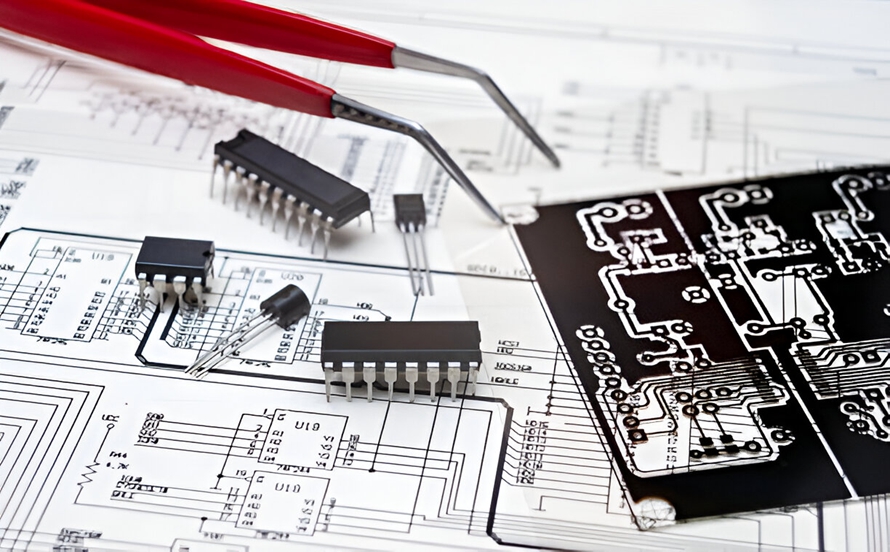
PCB technology has advanced significantly, enabling electronic products to become more functional, compact, durable, and faster. Modern devices such as smartphones, laptops, industrial controllers, automotive systems, and medical electronics all rely on printed circuit boards that go through systematic PCB Design, prototyping, manufacturing, assembly, and testing processes.
One common mistake in PCB Manufacturing and assembly is moving directly to mass production before the design and its manufacturing robustness have been sufficiently verified. A design may appear correct in simulation or on paper but still encounter problems during fabrication, assembly, testing, or real-world operation.
This is why PCB Prototyping is an important stage between design and production. It provides a practical way to manufacture, assemble, test, and evaluate a physical version of a PCB before committing to larger production volumes.
So, what is PCB prototyping? It is the structured process of creating and validating a physical PCB sample to identify design, manufacturing, assembly, and functional problems as early as possible.
What Is PCB Prototyping?
PCB Prototyping is the process of producing and testing a physical prototype based on a PCB design before proceeding to full-scale production.
A typical prototype may include PCB fabrication, component assembly, electrical testing, functional verification, and design iteration. Depending on the project, prototypes can be produced internally or by a specialized PCB manufacturer or assembly provider.
The primary purpose is not simply to produce a small number of boards. Instead, PCB prototyping is intended to verify whether the design can:
- Perform its intended electrical functions
- Be manufactured reliably
- Be assembled efficiently
- Meet mechanical requirements
- Meet thermal requirements
- Satisfy applicable design and manufacturing constraints
- Achieve the required performance in real-world testing
By identifying problems at an early stage, companies can avoid expensive design changes, material waste, production delays, and large quantities of defective products during mass production.
What Are the Steps in PCB Prototyping?
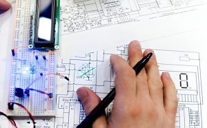
PCB prototyping involves multiple interconnected stages. Engineers, designers, procurement teams, PCB manufacturers, and assembly providers may all contribute to the process.
The exact workflow varies according to product complexity, but a typical PCB Prototype Process includes the following steps.
1. Define Project Requirements
The first step is to establish the technical and commercial requirements of the PCB.
Engineers should define:
- Intended functions
- Electrical specifications
- Operating voltage and current
- Signal requirements
- Board dimensions
- Component requirements
- Environmental conditions
- Thermal requirements
- Expected production volume
- Target cost
- Applicable standards and regulations
Clearly defined requirements provide a foundation for the subsequent PCB Design process.
Poorly defined requirements can lead to unnecessary redesigns later, so important electrical, mechanical, and manufacturing constraints should be identified as early as possible.
2. Create the PCB Schematic
Once the requirements have been established, engineers create the electronic schematic.
PCB design software such as Altium Designer, Autodesk Fusion, KiCad, and other EDA platforms can be used to place components and define their electrical connections.
The schematic establishes the logical relationships between:
- Integrated circuits
- Resistors
- Capacitors
- Diodes
- Transistors
- Connectors
- Sensors
- Power devices
- Other electronic components
The schematic is the foundation for the subsequent PCB layout. It should therefore be carefully reviewed before physical routing begins.
3. Create the Bill of Materials
The Bill of Materials (BOM) identifies the components required to build the PCB.
A production-oriented BOM may include:
- Manufacturer part number
- Component description
- Quantity
- Package type
- Approved supplier
- Reference designator
- Component value
- Alternative or substitute parts where appropriate
Component availability should be considered during prototyping. A theoretically suitable component may not be practical if it has long lead times, limited availability, or has already reached end-of-life status.
Identifying suitable alternatives early can reduce supply-chain risks during later production.
4. Develop the PCB Layout
After the schematic and component requirements have been established, engineers convert the electrical design into a physical PCB Layout.
The PCB layout defines:
- Board outline
- Component locations
- Copper traces
- Vias
- Copper planes
- Mounting holes
- Connectors
- Silkscreen information
- Solder-mask openings
Component placement should consider electrical performance, thermal management, mechanical constraints, assembly requirements, and serviceability.
For example, high-speed components should generally be positioned to minimize unnecessary signal-path length, while heat-generating components may require additional copper area or thermal structures.
The PCB layout should also be designed with the eventual PCB Manufacturing and PCB assembly processes in mind.
5. Perform Design Rule Checks
Design Rule Check (DRC) is an important verification step before manufacturing.
A DRC can identify violations such as:
- Insufficient trace spacing
- Incorrect trace widths
- Inadequate clearances
- Improper via dimensions
- Missing connections
- Clearance violations
- Other layout-rule problems
However, passing DRC does not automatically mean that a PCB design is electrically or functionally correct. Engineers should also perform schematic reviews, signal-integrity analysis, power analysis, mechanical checks, and other appropriate engineering verification.
6. Generate PCB Manufacturing Files
After the design has been verified, manufacturing documentation is generated.
Common fabrication data includes:
- Gerber files or other accepted artwork formats
- NC drill files
- Board fabrication drawings
- Stackup information
- Fabrication notes
- Material specifications
Assembly documentation is separate and may include:
- BOM
- Pick-and-place files
- Assembly drawings
- Assembly notes
Gerber files primarily describe PCB fabrication artwork such as copper, solder mask, and silkscreen layers. They do not by themselves contain all component procurement or assembly information.
7. Fabricate the PCB Prototype
The manufacturing files are provided to a PCB fabrication facility to produce the physical prototype.
A typical multilayer PCB Manufacturing Process may involve several major stages.
Lamination
Multilayer PCBs are constructed by combining copper foils, cores, and prepreg materials under controlled heat and pressure.
The core is a fully cured laminate, while prepreg is a partially cured resin-and-glass material used to bond layers together during lamination.
Drilling
Mechanical or laser drilling is used to create holes required by the design.
Depending on the PCB structure, these may include:
- Through-holes
- Blind vias
- Buried vias
- Microvias
Hole size and drilling method depend on the board design, layer structure, material, and manufacturer’s capabilities.
Imaging and Etching
The required copper pattern is transferred onto the PCB and unwanted copper is removed through controlled processing.
This creates the conductive traces and copper features specified by the design.
Solder Mask
Solder mask is applied to protect exposed copper and reduce the risk of unintended solder bridges during assembly. The areas that need to be soldered are selectively exposed through solder-mask openings.
Surface Finish
A surface finish is applied to exposed copper pads to improve solderability and protect the copper surface.
Common finishes include:
- HASL
- ENIG
- OSP
- Immersion tin
- Immersion silver
- ENEPIG
The appropriate finish depends on the application, assembly process, reliability requirements, and cost considerations.
Silkscreen
Reference designators, polarity indicators, labels, and other markings can be printed on the PCB to support assembly, inspection, and servicing.
Bare PCB Testing
Before component assembly, the fabricated board may undergo bare-board testing to identify manufacturing defects such as unintended opens and shorts.
Testing the bare PCB before assembly helps prevent defective boards from proceeding to the more expensive component assembly stage.
8. Assemble the PCB Prototype
Once the bare PCB passes the required fabrication inspections, electronic components can be assembled.
A typical prototype PCB Assembly process may include the following stages.
Solder Paste Printing
For SMT assembly, solder paste is deposited onto the appropriate PCB pads using a stencil or controlled dispensing method.
The stencil aperture design must correspond to the component footprints and assembly requirements.
Component Placement
Components are positioned according to the PCB layout.
For modern assemblies, pick-and-place machines can automatically place a large number of SMD components with high repeatability.
Through-hole components may be inserted manually or using automated insertion equipment, depending on the prototype volume and component type.
Reflow Soldering
For SMT components, the populated PCB passes through a reflow oven.
The board is heated according to a controlled thermal profile so that the solder paste melts, wets the component terminals and PCB pads, and then solidifies to create electrical and mechanical connections.
The thermal profile should be appropriate for the solder alloy, PCB materials, and component specifications.
Visual and Automated Inspection
After soldering, the prototype should be inspected for defects such as:
- Solder bridges
- Insufficient solder
- Component misalignment
- Missing components
- Incorrect component orientation
- Tombstoning
- Damaged components
Depending on the assembly, AOI and X-ray inspection may also be used.
X-ray inspection is particularly useful for inspecting hidden solder joints that cannot be adequately evaluated through conventional visual inspection.
9. Test the PCBA
After assembly, the completed PCBA must be tested to determine whether it meets the original design requirements.
Testing may include:
- Continuity testing
- Voltage testing
- Current testing
- Clock-signal verification
- Communication-interface testing
- In-circuit testing
- Functional testing
- Thermal testing
- Mechanical verification
The exact testing strategy depends on the PCB’s function and application.
If the prototype fails during testing, engineers can investigate whether the root cause is related to the schematic, PCB layout, component selection, fabrication, assembly, software, or another system-level issue.
This makes testing one of the most important stages of the PCB Prototyping process.
10. Iterate and Refine the PCB Design
PCB prototyping is rarely a one-time process, especially for new or technically complex products.
The prototype evaluation may reveal problems such as:
- Incorrect component values
- PCB layout limitations
- Signal-integrity issues
- Thermal problems
- Mechanical interference
- Assembly difficulties
- Connector-placement problems
- Unexpected electrical behavior
Engineers can then modify the PCB Design, manufacture another prototype, and repeat the testing process.
This design-build-test-revise cycle continues until the product meets the required technical and manufacturing objectives.
The goal is not simply to make one working board. The goal is to create a design that can be manufactured consistently and economically.
What Are the Benefits of PCB Prototyping?
Although PCB prototyping requires additional time and resources, it can significantly reduce risk before mass production.
Higher Production Yield
A prototype provides an opportunity to identify manufacturing and assembly problems before they affect a large production batch.
By resolving problems during the development stage, engineers can improve the manufacturability and assembly robustness of the final design.
Improved Product Quality
Prototype evaluation allows engineers to compare actual results against technical specifications and design requirements.
If a problem is identified, the team can investigate the underlying cause and improve the design, materials, manufacturing process, or assembly process.
This can contribute to better consistency and reliability in later production.
Faster Time to Market
Although prototyping takes additional time, finding problems early can reduce the amount of redesign and rework required later.
A validated prototype provides valuable information for finalizing the product before large-scale manufacturing begins.
This can reduce unexpected delays during production ramp-up.
Lower Overall Cost
Skipping prototyping may appear to save money initially, but undetected design problems can become significantly more expensive after mass production begins.
A prototype can help identify problems before large quantities of PCBs and components have been purchased or assembled.
It can therefore reduce the financial impact of:
- Large-scale rework
- Material waste
- Production downtime
- Engineering changes
- Product recalls
- Manufacturing scrap
PCB Prototyping vs Mass Production
PCB prototyping and mass production have different objectives.
| Factor | PCB Prototyping | Mass Production |
|---|---|---|
| Primary Goal | Validate the design | Produce consistent commercial products |
| Production Volume | Low | Medium to high |
| Design Changes | Frequent | Minimized after release |
| Testing | Focused on validation and troubleshooting | Standardized production testing |
| Manufacturing Optimization | Under development | Fully established |
| Assembly Process | May be flexible | Highly controlled and repeatable |
| Cost Focus | Design validation | Unit-cost optimization |
| Main Risk | Unidentified design problems | Production variation and yield loss |
A successful prototype provides the foundation for moving from development into controlled production.
Common PCB Prototyping Mistakes
Several mistakes can reduce the effectiveness of PCB prototyping.
Skipping the Prototype Stage
Moving directly to mass production without sufficient physical validation increases the risk of discovering expensive problems late in the product lifecycle.
Ignoring DFM Requirements
A PCB may work electrically but still be difficult or expensive to manufacture.
Design for Manufacturing (DFM) should therefore be considered before fabrication.
Using Unverified Component Footprints
An incorrect footprint can result in component misalignment, poor soldering, or mechanical interference. Footprints should be checked against the manufacturer’s datasheet and recommended land pattern.
Failing to Test the Complete System
A PCB that passes basic electrical tests may still fail under actual operating conditions.
Functional, thermal, mechanical, and interface testing should be considered according to the product’s requirements.
Treating the First Prototype as the Final Design
The purpose of prototyping is to learn from the physical implementation.
If testing reveals problems, the design should be revised and validated again rather than assuming that the first prototype is production-ready.
When Should You Move From PCB Prototyping to Production?
The transition to production should occur after the design has achieved an appropriate level of validation.
Before starting larger-scale PCB Manufacturing, engineers should ideally confirm:
- Electrical functionality
- Mechanical fit
- Thermal performance
- Component availability
- Manufacturing feasibility
- Assembly feasibility
- Test coverage
- Regulatory requirements where applicable
- Production documentation
- Target cost and yield expectations
At this stage, the PCB design should also be reviewed for DFM and DFA so that the prototype can be converted into a repeatable production process.
Conclusion
PCB Prototyping is a critical stage in modern electronic product development. It transforms a theoretical PCB Design into a physical, assembled, and tested product sample, allowing engineers to identify design, manufacturing, assembly, and functional problems before committing to large-scale production.
A typical PCB prototype process includes requirements planning, schematic development, BOM preparation, PCB layout, design verification, manufacturing-file generation, PCB fabrication, assembly, testing, and design iteration.
The real value of prototyping is not simply producing a sample board. It is reducing uncertainty and improving the design before production resources are committed on a larger scale.
Once the prototype has been successfully validated, the design can move into a controlled PCB Manufacturing and PCB Assembly process with greater confidence in its manufacturability, functionality, and reliability.