15 Best PCB Design Software for Professional PCB Design and Manufacturing
As modern electronic products become increasingly compact, powerful, and complex, printed circuit board (PCB) designs are becoming more densely populated and technically demanding. As a result, professional PCB Design software has become an essential tool for experienced engineers, PCB designers, and electronics development teams.
Choosing the right PCB design software can have a significant impact on design accuracy, engineering productivity, signal integrity, manufacturability, and overall product development efficiency. Modern PCB design tools allow engineers to create detailed schematics, place components, route traces, manage design constraints, verify electrical rules, visualize boards in 3D, and prepare manufacturing data.
Different PCB design platforms target different users and applications. Some focus on professional high-speed PCB design, while others are designed for beginners, educational projects, rapid prototyping, or open-source development.
This guide introduces 15 widely used PCB design software solutions and compares their major capabilities, advantages, limitations, and typical applications. It also explains how to select the right PCB design tool for your project and how software selection can affect the transition from PCB Design to PCB Manufacturing.
PCB Design Software Selection Guide
Before choosing a PCB design tool, engineers should evaluate the software according to project requirements, design complexity, team workflow, manufacturing requirements, and budget.
A professional PCB design platform should ideally provide an integrated workflow covering schematic capture, component management, PCB layout, routing, design-rule checking, visualization, documentation, and manufacturing output.
Constraint Management and Design Rule Checking
Design constraints and Design Rule Checking (DRC) are essential for maintaining electrical performance and manufacturability.
A capable PCB design tool should allow engineers to define trace widths, clearances, via sizes, differential-pair requirements, impedance constraints, component spacing, layer-specific rules, and other manufacturing requirements.
These rules help identify potential problems before the design reaches the manufacturing stage.
Advanced Routing
Modern electronic products often require high-speed interfaces, differential pairs, controlled impedance, and dense component placement.
Advanced routing features such as differential-pair routing, length tuning, interactive routing, impedance control, high-density interconnect (HDI) support, and automated routing can significantly improve design efficiency.
3D Modeling and Visualization
3D PCB visualization allows designers to inspect the physical appearance of a completed board and evaluate component clearances.
It is particularly useful for verifying the mechanical relationship between the PCB, connectors, heatsinks, enclosures, and other mechanical components.
For complex products, integrated ECAD-MCAD workflows can reduce mechanical interference and minimize late-stage design changes. Autodesk Fusion, for example, integrates PCB design with mechanical design within a unified environment.
Component and Library Management
A comprehensive component library is another important factor.
Engineers should be able to access verified symbols, footprints, 3D models, and component information while also creating and maintaining customized libraries.
Good library management can reduce repetitive work and lower the risk of incorrect footprints or component information.
Unified Design Environment
A unified environment connecting schematic capture and PCB layout can make the design process more efficient.
The ability to synchronize schematic and PCB data helps engineers maintain design consistency when components, connections, or board layouts are modified.
15 Best PCB Design Software for Professional Circuit Board Design
There is no single PCB design tool that is perfect for every project. The best choice depends on board complexity, required features, engineering experience, collaboration requirements, and budget.
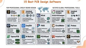
The following 15 PCB design software solutions represent a range of professional, commercial, open-source, cloud-based, and educational tools.
1. Altium Designer
Altium Designer is a professional PCB design platform widely used for complex electronic product development. It provides an integrated environment covering schematic capture, PCB layout, routing, simulation, documentation, and manufacturing outputs.
Its unified design environment, advanced routing capabilities, 3D visualization, design-rule management, and extensive component management make it suitable for demanding PCB projects. Altium’s current documentation also highlights advanced routing, rigid-flex design, simulation, 3D clearance checking, multi-board design, and manufacturing-release tools.
Advantages:
- Unified schematic and PCB design environment
- Advanced high-speed PCB design capabilities
- Powerful routing and constraint management
- 3D visualization and clearance checking
- Extensive component and design-management features
- Strong support for complex and multilayer designs
Limitations:
- Relatively high cost
- Steep learning curve for beginners
- Primarily associated with professional engineering workflows
Best for: Complex multilayer, high-speed, rigid-flex, and production-level PCB development.
2. Autodesk Fusion Electronics
Autodesk Fusion has become Autodesk’s primary direction for integrated electronics design following the retirement of EAGLE. Autodesk officially ended EAGLE sales and support on June 7, 2026, and recommends Fusion Electronics for continued PCB development.
Fusion Electronics combines schematic capture, PCB layout, 3D PCB visualization, mechanical design, simulation, and manufacturing workflows in a cloud-based product development environment.
Its ECAD-MCAD integration is particularly useful when PCB designers need to verify the relationship between the circuit board and mechanical enclosure.
Advantages:
- Integrated PCB and mechanical design
- 3D PCB visualization
- Cloud-based collaboration
- Schematic-to-PCB workflow
- Integrated simulation capabilities
- Strong ECAD-MCAD integration
Limitations:
- Subscription-based commercial model
- Cloud dependency for many workflows
- Some advanced enterprise PCB requirements may require more specialized tools
Best for: Product development teams that need PCB design and mechanical design in one environment.
3. KiCad
KiCad is a popular open-source PCB design suite that supports schematic capture, PCB layout, 3D visualization, and electrical rule checking.
It is available across major desktop operating systems and has developed into a capable solution for both hobbyist projects and increasingly sophisticated commercial PCB designs.
KiCad’s current platform includes an interactive router, integrated SPICE simulation, DRC, length tuning, 3D visualization, and migration support for several other PCB CAD formats.
Advantages:
- Open-source
- No conventional commercial license cost
- Cross-platform
- Integrated schematic and PCB design
- Powerful interactive routing
- 3D PCB visualization
- Large community and extensive libraries
Limitations:
- Some enterprise collaboration features are less extensive than those of major commercial platforms
- Advanced workflows may require more manual configuration
- Beginners may need time to learn the interface
Best for: Open-source projects, startups, education, prototyping, and engineers looking for a powerful free PCB design solution.
4. Cadence OrCAD X
OrCAD is a professional PCB design platform from Cadence and is widely associated with schematic capture, PCB layout, simulation, constraint-driven design, and engineering analysis.
It is particularly suitable for engineers working on complex boards where electrical performance, design rules, and verification are important.
Advantages:
- Professional schematic and PCB layout capabilities
- Constraint-driven design
- High-speed routing support
- Simulation and analysis capabilities
- Suitable for complex multilayer PCB designs
Limitations:
- Commercial licensing can be expensive
- Advanced functions require engineering experience
- More complex than entry-level PCB tools
Best for: Professional electronics development, high-speed PCB design, industrial electronics, and demanding engineering applications.
5. DipTrace
DipTrace is a PCB design platform known for its relatively accessible interface and integrated schematic, PCB layout, and library management tools.
It is often considered by engineers, small businesses, startups, and designers who need professional PCB design capabilities without the complexity of some enterprise-level platforms.
Advantages:
- User-friendly interface
- Integrated schematic and PCB layout
- Extensive component libraries
- Automatic routing capabilities
- Suitable for small and medium-sized projects
Limitations:
- Simulation capabilities are less extensive than some high-end platforms
- Advanced enterprise features are more limited
- High-end high-speed workflows may require more specialized software
Best for: Small and medium-sized PCB projects and engineers seeking a balance between usability and functionality.
6. EasyEDA
EasyEDA is a browser-based and desktop-supported EDA platform designed to simplify schematic capture, PCB layout, simulation, component management, and manufacturing preparation.
Its combination of an accessible interface, extensive component libraries, cloud collaboration, PCB design tools, and manufacturing integration makes it popular among students, makers, engineers, and rapid-prototyping teams.
EasyEDA currently provides both Standard and Pro editions, with features including DRC, Gerber generation, 3D visualization, blind and buried vias, routing, and library management.
Advantages:
- Easy to learn
- Browser-based workflow
- Desktop application available
- Large component library
- PCB layout and schematic integration
- Gerber manufacturing output
- Convenient for rapid prototyping
Limitations:
- Cloud-oriented workflows may not suit every organization
- Advanced professional requirements may require the Pro edition
- Some teams may prefer fully local enterprise EDA environments
Best for: Rapid prototyping, education, makers, startups, and small-to-medium PCB projects.
7. Proteus
Proteus is an electronics design and simulation platform that combines circuit simulation with PCB design capabilities.
One of its major strengths is virtual prototyping, which allows designers and students to simulate circuits before producing physical hardware.
Advantages:
- Strong circuit simulation capabilities
- Virtual prototyping
- PCB design functionality
- Useful for education and embedded-system development
- Interactive simulation environment
Limitations:
- Some advanced PCB workflows are less extensive than those in high-end professional EDA platforms
- Complex projects may require additional engineering tools
- Learning advanced simulation features can take time
Best for: Education, embedded-system development, circuit simulation, and small PCB projects.
8. CircuitMaker
CircuitMaker is an Altium-developed PCB design platform aimed primarily at makers, hobbyists, and collaborative electronics development.
It provides a modern design environment with access to PCB design functions and community-oriented workflows.
Advantages:
- Accessible PCB design environment
- Community-oriented workflow
- Modern interface
- Suitable for hobbyists and makers
- Useful PCB layout capabilities
Limitations:
- Community and cloud-based workflows may not fit every professional organization
- Advanced enterprise capabilities are more limited
- Internet connectivity may be required for some functions
Best for: Makers, hobbyists, students, and collaborative PCB development.
9. PADS Professional
PADS Professional is a PCB design solution from Siemens designed for professional hardware engineers and small-to-medium design teams.
It provides schematic and PCB layout functionality, constraint management, ECAD-MCAD collaboration, simulation options, and cloud-connected capabilities.
Siemens currently positions PADS Professional as an established solution while encouraging new users to explore Xpedition Standard as its next-generation, upward-compatible path.
Advantages:
- Suitable for complex PCB designs
- Constraint management
- ECAD-MCAD collaboration
- Professional PCB layout capabilities
- Cloud-connected options
- Design-to-production workflow
Limitations:
- Requires time to learn
- Commercial licensing
- Some new users may need to evaluate Xpedition Standard for future scalability
Best for: Professional engineering teams and users working within the Siemens EDA ecosystem.
10. Autodesk Fusion Electronics
Fusion Electronics provides an integrated environment for schematic design, PCB layout, 3D PCB visualization, simulation, and mechanical product development.
The electronics workflow connects schematic, 2D PCB, and 3D PCB documents, allowing engineers to work across electrical and mechanical aspects of product design.
Advantages:
- Integrated ECAD-MCAD workflow
- Strong 3D visualization
- Mechanical enclosure integration
- Cloud collaboration
- PCB and manufacturing workflow integration
- Simulation capabilities
Limitations:
- Subscription-based
- Cloud-oriented workflow
- May require time to learn the broader Fusion environment
Best for: Product teams designing complete electronic products that combine PCB and mechanical engineering.
Note: Because Autodesk EAGLE reached end-of-life in June 2026, current articles should refer to Autodesk Fusion Electronics rather than presenting EAGLE as an actively supported standalone PCB design platform.
11. DesignSpark PCB
DesignSpark PCB is designed to provide an accessible PCB design environment for engineers, makers, educators, and small businesses.
It offers schematic capture, PCB layout, component libraries, and 3D visualization.
Advantages:
- Easy to learn
- Accessible interface
- Component library support
- 3D visualization
- Suitable for basic and intermediate PCB designs
Limitations:
- Advanced capabilities are more limited than high-end commercial EDA tools
- Automation and advanced routing may be less sophisticated
- Technical support options can vary
Best for: Beginners, makers, educators, and small PCB projects.
12. NI Multisim
NI Multisim is primarily known for circuit simulation and virtual instrumentation rather than being a complete high-end PCB layout platform.
It is widely used in education, training, and engineering environments where circuit behavior needs to be simulated and analyzed before hardware implementation.
Advantages:
- Strong SPICE-based simulation
- Virtual instruments
- User-friendly interface
- Excellent for education and circuit analysis
- Useful for testing circuit behavior before PCB implementation
Limitations:
- Not primarily a complete modern PCB layout solution
- Specialized component availability can vary
- Commercial versions can be expensive
Best for: Education, circuit simulation, laboratory work, and pre-PCB circuit verification.
13. ExpressPCB
ExpressPCB is a straightforward PCB design tool intended for users who want a relatively simple workflow for creating circuit boards.
Its accessible interface makes it suitable for beginners and basic prototyping projects.
Advantages:
- Easy to learn
- Simple interface
- Suitable for basic PCB projects
- Convenient for rapid prototyping
Limitations:
- Limited advanced PCB design features
- Less suitable for highly complex multilayer boards
- Library capabilities are more limited than those of major professional EDA platforms
Best for: Beginners, hobbyists, and simple prototype PCB projects.
14. Xpedition Standard
Xpedition Standard is part of Siemens’ modern PCB design portfolio and is positioned as an evolution of the PADS workflow.
It is designed for individual engineers and small teams that need a more scalable PCB development environment as design complexity increases.
Siemens describes Xpedition Standard as a next-generation solution built on Xpedition technology, with capabilities including PCB layout, constraint management, ECAD-MCAD co-design, DFM analysis, collaboration, and AI-enabled workflows.
Advantages:
- Modern PCB design environment
- Scalable for growing design complexity
- Constraint management
- ECAD-MCAD co-design
- DFM capabilities
- Collaboration and supply-chain features
Limitations:
- Commercial platform
- More appropriate for professional engineering users
- May be more functionality than required for simple hobby projects
Best for: Professional engineers and teams looking for a scalable Siemens EDA PCB design workflow.
15. LibrePCB
LibrePCB is an open-source PCB design application focused on providing a straightforward and accessible workflow for schematic and PCB development.
It can be an attractive option for users who prefer open-source software and want a lightweight alternative for electronic design projects.
Advantages:
- Open-source
- Accessible interface
- Suitable for learning and prototyping
- No traditional commercial license
- Community-oriented development
Limitations:
- Smaller ecosystem than major commercial EDA platforms
- Fewer advanced enterprise capabilities
- Not intended to replace every high-end professional PCB design workflow
Best for: Learning, open-source projects, hobby electronics, and lightweight PCB development.
Top PCB Design Software Comparison
Each PCB design tool has different strengths and limitations. Instead of choosing software based only on popularity or price, engineers should evaluate how well the tool supports their actual design workflow.
| Software | Difficulty | Advanced Routing | Simulation | Best For | Cost Model |
|---|---|---|---|---|---|
| Altium Designer | Advanced | Excellent | Yes | Complex, high-speed PCB design | Commercial subscription |
| Autodesk Fusion Electronics | Moderate | Advanced | Yes | ECAD-MCAD product development | Subscription |
| KiCad | Moderate | Advanced | Yes | Open-source and professional PCB design | Free/Open Source |
| OrCAD X | Advanced | Advanced | Yes | High-speed and professional PCB design | Commercial |
| DipTrace | Moderate | Advanced | Limited | Small and medium-sized projects | Commercial |
| EasyEDA | Easy–Moderate | Advanced | Yes | Rapid prototyping and cloud PCB design | Free + paid options |
| Proteus | Moderate | Moderate | Excellent | Simulation and education | Commercial |
| CircuitMaker | Easy–Moderate | Moderate | Limited | Makers and collaborative projects | Free |
| PADS Professional | Advanced | Advanced | Yes | Professional engineering teams | Commercial |
| DesignSpark PCB | Easy–Moderate | Moderate | Limited | Beginners and small businesses | Free/Paid options |
| NI Multisim | Moderate | Limited | Excellent | Education and circuit simulation | Commercial |
| ExpressPCB | Easy | Basic | Limited | Basic PCB prototyping | Free/Paid options |
| Xpedition Standard | Advanced | Advanced | Yes | Professional and scalable PCB design | Commercial |
| LibrePCB | Easy–Moderate | Basic–Moderate | Limited | Open-source and learning | Free/Open Source |
How to Choose the Right PCB Design Software
Selecting the right PCB design software requires more than comparing feature lists. Engineers should consider the complete product development process, from schematic design to PCB Manufacturing.
1. Consider Ease of Use
A complicated software interface can increase development time, especially for beginners.
The ideal tool should make schematic capture, component placement, routing, design-rule checking, and documentation straightforward.
For beginners, KiCad, EasyEDA, DesignSpark PCB, and other accessible tools may provide a gentler learning curve.
For experienced engineers designing complex products, advanced professional platforms may offer more powerful capabilities even if they require more training.
2. Evaluate Your Budget
PCB design software ranges from free open-source solutions to expensive professional platforms.
Free tools such as KiCad can be attractive for students, startups, hobbyists, and open-source projects.
Professional platforms may require subscriptions or commercial licenses, but they can provide advanced routing, simulation, collaboration, component management, and engineering support.
The total software cost should therefore be evaluated together with the time saved during design and debugging.
3. Match the Software to Project Complexity
A simple single-sided PCB does not require the same capabilities as a high-speed multilayer PCB.
For simple boards, basic schematic and PCB layout tools may be sufficient.
For complex designs, engineers may need:
- High-speed routing
- Differential-pair routing
- Length matching
- Controlled impedance
- Advanced layer-stack management
- HDI support
- Rigid-flex design
- Signal integrity analysis
- Power integrity analysis
- Thermal analysis
- Advanced DRC
- ECAD-MCAD integration
Choosing software based on the actual technical requirements can prevent unnecessary limitations later in the development cycle.
4. Check Component Libraries
A large and well-maintained component library can significantly accelerate PCB development.
Engineers should check whether the software provides reliable symbols, footprints, 3D models, manufacturer information, and customizable library tools.
Library accuracy is particularly important because an incorrect footprint can cause serious PCB assembly and manufacturing problems.
5. Consider Manufacturing Compatibility
PCB design does not end when the layout is completed.
The design must eventually be converted into manufacturing data such as Gerber files, drill files, pick-and-place files, BOMs, and other production documentation.
A good PCB design tool should therefore provide a reliable path from design to manufacturing.
For example, EasyEDA supports Gerber generation and other manufacturing outputs directly within its workflow.
6. Consider Collaboration and Data Management
For professional engineering teams, collaboration can be just as important as PCB layout capabilities.
Cloud-based platforms can provide version management, centralized project data, team collaboration, and supply-chain information.
However, companies handling sensitive product designs should also evaluate data-security requirements, access controls, cloud policies, and internal compliance requirements.
PCB Design Software and PCB Manufacturing
The PCB design software you select can directly affect the efficiency of the manufacturing process.
A well-designed PCB should not only satisfy electrical requirements but also be manufacturable and assemblable.
During the design stage, engineers should consider:
- Minimum trace width and spacing
- Via diameter and aspect ratio
- Layer stackup
- Copper thickness
- PCB material
- Controlled impedance
- Component spacing
- Solder mask requirements
- Silkscreen clearance
- Board-edge clearance
- Panelization
- Surface finish
- DFM requirements
- PCB assembly requirements
Design Rule Checking and Design for Manufacturing (DFM) analysis can identify potential problems before the PCB enters production.
This is particularly important for high-density boards, HDI PCBs, high-speed designs, rigid-flex PCBs, and other technically demanding products.
The final design should be reviewed against the capabilities of the selected PCB manufacturer before manufacturing files are released.
PCB Design Software FAQs
What is PCB design software?
PCB design software is an electronic design automation (EDA) tool used to create circuit schematics, PCB layouts, component placements, copper routing, design rules, and manufacturing documentation.
Modern PCB design platforms can also provide simulation, 3D visualization, library management, collaboration, and manufacturing preparation.
What is the best free PCB design software?
KiCad is one of the most widely used open-source PCB design solutions. It provides schematic capture, PCB layout, DRC, interactive routing, SPICE simulation, and 3D visualization.
EasyEDA also provides free PCB design capabilities and browser-based access, making it another option for users who prioritize accessibility and rapid prototyping.
Is Altium Designer suitable for professional PCB design?
Yes. Altium Designer provides an integrated professional environment covering schematic capture, PCB layout, routing, simulation, 3D visualization, design management, and manufacturing outputs.
Is Autodesk EAGLE still available?
Autodesk EAGLE is no longer an actively supported solution. Autodesk ended EAGLE sales and support on June 7, 2026, and directs users toward Autodesk Fusion Electronics.
Can PCB design software generate manufacturing files?
Yes. Many modern PCB design platforms can generate Gerber files, drill files, BOMs, pick-and-place data, and other manufacturing outputs required for PCB fabrication and assembly.
However, engineers should always verify the generated files using a Gerber viewer and review them against the manufacturer’s fabrication and assembly capabilities before production.
Conclusion
Selecting the right PCB design software is an important part of developing reliable and manufacturable electronic products.
The right tool can improve schematic capture, component placement, routing, design-rule checking, simulation, 3D visualization, collaboration, and manufacturing preparation. However, the most suitable software depends on the complexity of the project, engineering requirements, team size, budget, and manufacturing workflow.
For advanced professional designs, engineers may require sophisticated tools such as Altium Designer, OrCAD X, PADS Professional, or Xpedition Standard. For open-source development and cost-sensitive projects, KiCad provides a powerful alternative. EasyEDA and Autodesk Fusion Electronics can be attractive for rapid prototyping and integrated product development, while Proteus and NI Multisim are particularly useful when circuit simulation and education are important.
Most importantly, PCB design software should be evaluated not only by its design features but also by how efficiently it supports the complete path from PCB Design to PCB Manufacturing.
After completing the design, choosing an experienced PCB manufacturing and assembly partner is equally important. Kingda provides professional PCB manufacturing and PCB assembly services to help engineers transform PCB designs into reliable production-ready circuit boards.