Stamp Hole Probe: A Key Tool for High-Precision PCB Testing
In modern electronics manufacturing, reliable electrical testing is essential for verifying PCB connectivity, assembly quality, and functional performance. A Stamp Hole Probe provides a practical test interface by contacting dedicated PCB test points or plated holes and transmitting electrical signals to the testing system.
When properly designed and integrated into a test fixture, a PCB Test Probe can provide stable contact, repeatable measurements, and efficient test access without requiring permanent soldered connections. This makes probe-based testing particularly useful for prototype validation, production inspection, and automated PCB Testing.
For manufacturers handling projects from prototypes to volume production, combining PCB fabrication, assembly, and testing within one manufacturing workflow can also simplify quality control and reduce supplier coordination. GOPCBA provides integrated PCB Manufacturing and PCBA services for different production requirements.
What Is a Stamp Hole Probe?
Definition and Function
A stamp hole probe is a precision electrical contact probe designed to connect a test fixture with a PCB test point, plated hole, or other designated electrical interface.
During testing, the probe is pressed against the corresponding PCB contact area. Its spring-loaded structure maintains contact pressure while the conductive tip transfers electrical signals between the PCB and the test equipment.
The basic testing process can be summarized as:
PCB Test Point → Probe Contact → Test Fixture → Measurement System
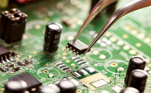
This structure allows engineers to measure electrical parameters without permanently modifying the assembled PCB.
How Does a Stamp Hole Probe Work?
A typical probe contains a conductive contact tip, spring mechanism, and outer body. When the fixture closes, mechanical pressure compresses the spring and pushes the probe tip against the PCB contact surface.
The spring compensates for small variations in PCB thickness, fixture height, and contact position. Stable mechanical pressure helps maintain consistent electrical contact during repeated testing.
For PCBA production, this principle is commonly incorporated into dedicated fixtures for ICT Testing and functional verification. GOPCBA’s published testing capabilities include ICT with more than 4,096 test points, along with contact testing, open/short testing, resistance-capacitance testing, boundary scan, and powered testing.
Key Technical Characteristics of PCB Test Probes
Stable Electrical Contact
The most important requirement of a PCB Test Probe is reliable electrical contact. The probe tip must maintain sufficient pressure against the test point while minimizing contact resistance.
A stable connection helps reduce intermittent failures and measurement variation, particularly when a fixture performs repeated testing on large production quantities.
Spring-Loaded Contact Structure
The internal spring allows the probe to accommodate small mechanical variations. Instead of requiring the PCB and fixture to have absolutely identical dimensions, the spring provides a degree of mechanical compensation.
Important design parameters include:
- Probe diameter
- Working stroke
- Spring force
- Contact-tip geometry
- Contact resistance
- Mechanical positioning accuracy
- Expected operating cycles
The correct combination depends on the PCB structure, test-point geometry, fixture design, and electrical requirements.
Conductive Contact Materials
Probe performance depends strongly on the materials used for the contact tip, spring, and body.
Common considerations include:
- Conductive alloys for the contact tip
- Gold or other protective plating for improved contact stability
- Spring materials with good fatigue resistance
- Insulating materials for electrical isolation
Material selection should consider current, voltage, frequency, environmental conditions, and expected test cycles rather than relying only on nominal probe dimensions.
Stamp Hole Probe Applications
ICT Testing
ICT Testing checks the electrical characteristics of a PCB or PCBA through multiple predefined test points.
A test fixture positions multiple probes over the board and establishes electrical connections with the circuit. The system can then perform tests such as:
- Continuity testing
- Open and short circuit detection
- Resistance measurement
- Capacitance measurement
- Component verification
- Boundary scan
- Powered electrical testing
This approach is particularly valuable for production environments where repeatable automated testing is required.
GOPCBA integrates ICT and other inspection methods into its PCBA quality process, including SPI, AOI, X-ray, FAI, and FCT.
Functional Testing
FCT Testing evaluates whether the assembled PCB operates according to its intended functional requirements.
Unlike basic connectivity testing, functional testing may involve powering the PCBA and verifying actual operating behavior, including:
- Voltage and current
- Digital signals
- Analog signals
- Communication interfaces
- Sensor responses
- Motor or actuator control
- Firmware operation
- User-interface functions
GOPCBA describes FCT as a method for verifying PCBA functionality and performance, making test-point and fixture design an important part of the overall manufacturing process.
Prototype and Engineering Debugging
Probe interfaces are also useful during prototype development because engineers can repeatedly access important circuit nodes without soldering test wires directly to the board.
This can simplify:
- Circuit debugging
- Voltage measurement
- Signal verification
- Firmware development
- Hardware validation
- Engineering modifications
For rapid development projects, probe-based interfaces can make repeated measurements faster and reduce unnecessary modification of prototype boards.
GOPCBA supports rapid PCBA prototyping and low-volume production, with testing options including ICT and FCT.
High-Density PCB Test Considerations
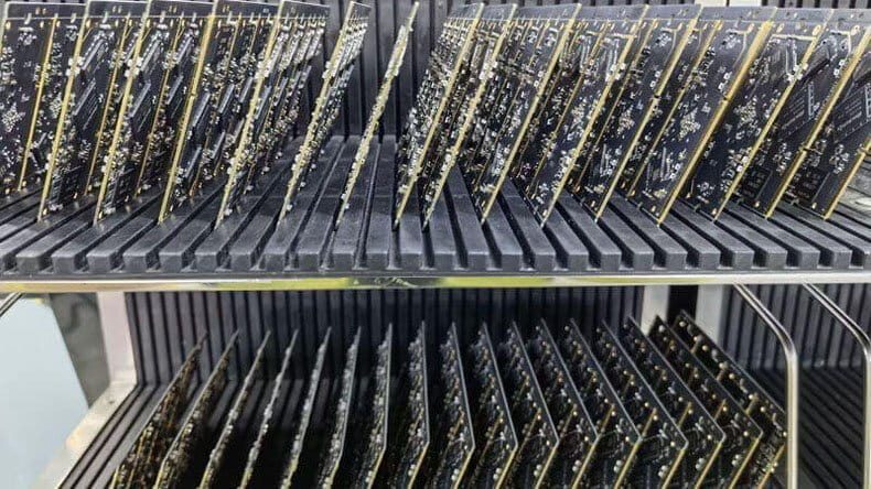
As PCB designs become smaller and more complex, test-point density becomes an important engineering consideration.
Smaller Probe Diameters
High-density boards may require smaller probes to fit within restricted test areas. However, reducing probe size can affect mechanical strength, current capacity, stroke, and durability.
Therefore, miniaturization should be evaluated together with the electrical and mechanical requirements of the test fixture.
Test Point Spacing
Probe spacing must correspond to the PCB layout and fixture structure. Insufficient clearance can result in mechanical interference or accidental contact between neighboring test points.
For high-density designs, test-point placement should therefore be considered during PCB layout rather than after the board has already been manufactured.
Signal Integrity
High-speed circuits require additional attention to the electrical characteristics of the test path. Probe geometry, fixture wiring, connector selection, grounding, and signal routing can all affect measurement quality.
For high-speed or high-frequency applications, the complete test path should be evaluated rather than considering the probe as an isolated component.
How to Select the Right PCB Test Probe
1. Match the Probe to the Test Point
The probe tip must be compatible with the size, shape, plating, and location of the PCB test point.
Consider:
- Test-point diameter
- Hole diameter
- Pad geometry
- Surface finish
- Available clearance
- PCB thickness
2. Select Appropriate Spring Force
Insufficient contact force may cause unstable electrical connections, while excessive force can damage pads, plated holes, or the PCB itself.
The selected spring force should therefore provide reliable contact without placing unnecessary mechanical stress on the board.
3. Consider Electrical Requirements
Probe selection should account for:
- Maximum current
- Operating voltage
- Contact resistance
- Signal frequency
- Insulation requirements
- Grounding requirements
For high-current applications, the contact structure and thermal behavior require particular attention.
4. Consider Service Life
Production fixtures may operate thousands or millions of test cycles. Probe selection should therefore consider mechanical durability, spring fatigue, contact-tip wear, and plating performance.
The expected service life should be evaluated against the actual production volume and fixture maintenance schedule.
PCB Test Fixture Design Considerations

Mechanical Alignment
Accurate alignment between the PCB and probe array is essential. Fixture positioning pins, support structures, and guide mechanisms should keep the PCB stable during testing.
Poor alignment can cause inconsistent contact or damage to test pads.
PCB Support
The PCB should be adequately supported, especially when many probes are applied simultaneously.
Proper support helps prevent:
- PCB bending
- Pad damage
- Probe misalignment
- Uneven contact pressure
- Mechanical stress on components
Electrical Isolation
Adjacent test points may carry different signals or voltage levels. The fixture should provide sufficient electrical isolation to prevent unintended shorts.
Test-Point Layout
Test points should ideally be planned during PCB design. Appropriate positioning can make the fixture simpler, improve accessibility, and reduce testing costs.
For advanced PCB projects, manufacturing and testing requirements should be considered together during engineering review. GOPCBA provides PCB manufacturing, engineering support, and PCBA testing as part of its integrated manufacturing capabilities.
Stamp Hole Probe vs. Other PCB Test Interfaces
Different testing requirements may call for different contact methods.
| Test Interface | Main Advantage | Typical Application |
|---|---|---|
| Spring Probe | Fast and repeatable contact | ICT and FCT fixtures |
| Stamp Hole Probe | Convenient access through PCB holes | PCB test fixtures |
| Test Pad | Simple PCB interface | Electrical measurement |
| Connector Interface | Supports repeated connection | System-level testing |
| Soldered Test Wire | Flexible temporary access | Engineering debugging |
The best solution depends on the board design, testing frequency, signal requirements, and expected production volume.
PCB Testing Quality Control
A reliable test interface is only one part of an effective quality-control system. The PCB manufacturing and assembly process should also include appropriate inspection and verification procedures.
A comprehensive workflow may include:
Incoming Inspection → SMT/THT Assembly → SPI → AOI → X-Ray → ICT → FCT → Final Inspection
GOPCBA’s published PCBA process includes automated optical inspection, X-ray inspection, first article inspection, ICT, FCT, and other reliability testing capabilities.
For bare PCB production, electrical testing can also verify conductivity, insulation resistance, and circuit integrity before boards are shipped for assembly.
Best Practices for Using PCB Test Probes
Control Contact Pressure
Use the appropriate spring force and working stroke to achieve reliable contact without excessive mechanical loading.
Keep Contact Surfaces Clean
Dust, oxidation, solder residue, and contamination can increase contact resistance. Regular fixture and probe maintenance helps maintain stable testing performance.
Inspect Probe Wear
Production probes should be periodically inspected for:
- Worn tips
- Damaged springs
- Reduced contact force
- Corrosion
- Increased contact resistance
- Mechanical deformation
Design for Manufacturability and Testing
Test access should be considered during PCB layout and manufacturing engineering. Providing dedicated test points can make automated testing more reliable and reduce fixture complexity.
Why Test Probe Design Matters for PCBA Manufacturing
A PCB can be correctly fabricated and assembled yet still be difficult to test if test access was not considered during design.
An effective test strategy connects three areas:
PCB Design → PCBA Manufacturing → Test Engineering
Test points must be electrically meaningful, mechanically accessible, and positioned appropriately for the fixture.
This is especially important for high-density, multilayer, high-speed, and complex PCB assemblies where troubleshooting without dedicated test access can significantly increase engineering time.
For manufacturers seeking an integrated production process, GOPCBA combines PCB Assembly with component sourcing, SMT/THT assembly, inspection, testing, and final assembly.
Integrated PCB Manufacturing and Testing
For production projects, separating PCB fabrication, assembly, and testing across multiple suppliers can increase communication and quality-control complexity.
An integrated manufacturing workflow can instead connect:
PCB Manufacturing → Component Procurement → SMT/THT Assembly → Inspection → ICT/FCT → Final Inspection
This approach allows test requirements to be considered earlier in the manufacturing process and helps maintain better process continuity.
GOPCBA supports prototype, low-volume, and volume PCBA production and provides a combination of PCB fabrication, component procurement, assembly, inspection, and testing services.
Conclusion
A Stamp Hole Probe is a practical interface for establishing repeatable electrical contact between a PCB and a test fixture. Its performance depends on probe geometry, spring characteristics, contact materials, positioning accuracy, PCB test-point design, and fixture construction.
For reliable PCB Testing, engineers should select probes according to the electrical and mechanical requirements of the application rather than focusing only on probe size. Proper test-point planning, fixture alignment, contact-force control, and regular maintenance are equally important.
In automated production, ICT Testing and FCT Testing can work together to verify both electrical integrity and functional performance. A well-designed probe and fixture system can improve test repeatability, simplify troubleshooting, and support efficient PCB assembly quality control.
For projects requiring PCB fabrication, assembly, inspection, and testing under one manufacturing workflow, PCBA Testing Services can provide a more integrated approach from prototype validation through production testing.