PCB Copper Pour: Applications and Manufacturing Considerations
PCB copper pour is a common PCB layout and manufacturing technique in which large areas of copper are added to unused regions of a circuit board. Depending on the design, the copper area may be connected to ground, a power network, or another electrical net.
Copper pouring is widely used in multilayer and double-sided circuit boards because it can improve grounding, reduce ground impedance, support current distribution, improve heat dissipation, and help control electromagnetic interference. For complex boards, the relationship between copper areas, traces, vias, pads, and the PCB stack-up must be carefully considered during both design and manufacturing.
For projects requiring advanced fabrication capabilities, PCB manufacturing services can support different board structures, materials, copper weights, layer counts, and manufacturing requirements.
Where Is PCB Copper Pour Used?
The application of copper pour PCB technology depends largely on the electrical and thermal requirements of the circuit.
Common applications include:
- Power supply and power management circuits
- High-current electronic systems
- High-frequency and RF circuits
- Industrial control equipment
- Communication equipment
- Automotive electronics
- Battery management systems
- Energy storage equipment
- Thermal management structures
- Multilayer PCB ground and power planes
In high-current applications, large copper areas can provide lower-resistance current paths and distribute heat more effectively. In sensitive signal applications, properly designed ground planes can also provide a more stable return-current path and help reduce electromagnetic interference.
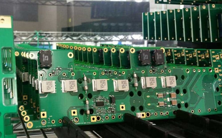
For example, high-power BMS designs may combine heavy copper structures with optimized current paths and thermal management to handle high current and reduce localized heating. GOPCBA’s BMS manufacturing experience includes heavy-copper designs and parallel-via structures for high-current applications.
PCB Copper Thickness and Copper Weight Selection
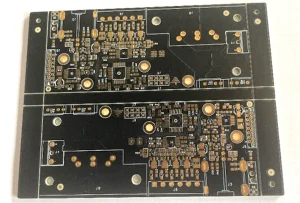
PCB copper thickness is normally specified either by physical thickness or by copper weight, such as oz/ft².
Typical copper weights include:
| Copper Weight | Approximate Copper Thickness | Typical Application |
|---|---|---|
| 0.5 oz | ~17 μm | Fine-pitch and standard signal circuits |
| 1 oz | ~35 μm | General-purpose PCB applications |
| 2 oz | ~70 μm | Higher-current and thermal applications |
| 3 oz | ~105 μm | High-current and power electronics |
| 4 oz+ | ~140 μm+ | Heavy-current and specialized applications |
The exact finished copper thickness depends on the fabrication process, plating, layer position, and manufacturer specifications. Designers should therefore distinguish between base copper thickness and finished copper thickness when establishing production requirements.
GOPCBA’s published manufacturing capabilities support copper weights up to 10 oz for PCB fabrication, depending on the board structure and manufacturing requirements.
How to Choose the Right Copper Thickness
Copper weight should not be selected simply because thicker copper appears to provide better performance. The appropriate value depends on:
- Required current capacity
- Allowable temperature rise
- Trace width
- Thermal dissipation requirements
- Layer count
- PCB thickness
- Via construction
- Minimum line and spacing requirements
- Manufacturing cost
- Mechanical requirements
For standard digital and control circuits, 1 oz copper is often sufficient. Higher copper weights become more useful when current levels, thermal loads, or mechanical requirements increase.
For projects involving demanding thermal or high-current conditions, heavy copper PCB manufacturing provides a more appropriate solution than simply increasing the copper area of a conventional PCB.
Special PCB Copper Pour Design Considerations
Copper pouring is not simply a matter of filling unused PCB space with copper. The copper area must be correctly connected, isolated, and integrated with the overall circuit design.
Irregular Copper Areas
PCB designs may require copper areas with irregular shapes because of component placement, mechanical openings, board outlines, or electrical isolation requirements.
The copper boundary should maintain an appropriate clearance from:
- Signal traces
- Pads
- Board edges
- Mounting holes
- Other copper networks
- Mechanical cutouts
The required clearance depends on the PCB manufacturing process and design rules. GOPCBA publishes specific copper-to-edge capabilities as part of its PCB manufacturing specifications.
Ground Plane and Power Plane Design
Ground copper pours are commonly used to create low-impedance return paths and improve power integrity.
In multilayer PCBs, dedicated ground and power planes can provide more predictable electrical performance than fragmented copper areas. A properly planned stack-up can also help control signal return paths and impedance.
For complex multilayer designs, PCB capabilities should be evaluated together with the required layer count, copper weight, dielectric structure, via technology, and minimum feature size.
Thermal Relief and Thermal Pads
When copper pours are connected directly to component pads, the large copper area can draw heat away rapidly during soldering. This may make soldering more difficult or create uneven heating.
Thermal relief connections use narrower copper spokes between the pad and surrounding copper area. This reduces heat transfer during soldering while maintaining electrical connectivity.
This approach is especially useful for:
- Ground pads
- Through-hole component pads
- Power components
- Large copper planes
- Components requiring controlled soldering conditions
The thermal design must balance electrical conductivity, heat dissipation, and assembly reliability.
Copper Pour and Via Connections
Vias can connect copper areas between different PCB layers, allowing ground or power networks to move vertically through the board.
For high-current applications, multiple vias may be placed in parallel to reduce current density and improve thermal transfer. However, via size, spacing, copper thickness, drilling capability, and plating requirements must all be considered.
Advanced PCB manufacturing can support technologies such as blind vias, buried vias, microvias, copper-filled vias, and via-in-pad structures when required by the design.
PCB Copper Pour for High-Current Applications
High-current circuits place greater demands on copper thickness, trace geometry, via structures, and thermal management.
Increasing copper weight can reduce conductor resistance and increase current-carrying capacity. A larger copper area can also distribute heat over a greater surface area, reducing localized thermal stress.
However, high-current PCB design should consider the complete electrical path rather than copper thickness alone.
Important factors include:
- Copper weight
- Trace width
- Current density
- Temperature rise
- Via quantity and construction
- Component thermal performance
- PCB material
- Layer stack-up
- Heat-sink integration
- Airflow and system-level cooling
GOPCBA’s published heavy-copper manufacturing information notes that heavy copper designs require additional process control because thicker copper affects etching, plating, line definition, hole filling, lamination, and dimensional control.
PCB Copper Pour for High-Frequency Circuits
In high-frequency circuits, copper pouring must be considered together with signal integrity and return-current behavior.
A continuous ground plane can provide a predictable return path and reduce unwanted loop area. However, improperly divided or interrupted copper can force return currents to take longer paths, potentially increasing electromagnetic coupling and signal integrity problems.
High-speed PCB designs therefore require careful coordination between:
- Copper plane structure
- Signal routing
- Impedance control
- Layer stack-up
- Dielectric thickness
- Via placement
- Ground stitching
- Copper surface characteristics
For high-speed applications, high-speed PCB manufacturing requires close attention to stack-up, impedance, registration, copper plating, and signal integrity.
PCB Copper Pour in Multilayer Boards
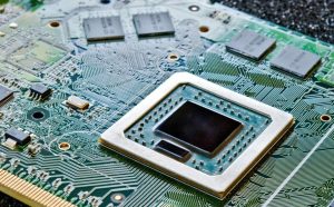
In multilayer PCBs, copper planes can serve different electrical functions on different layers.
A typical multilayer structure may include:
- Top signal layer
- Ground plane
- Power plane
- Internal signal layers
- Additional ground or power planes
- Bottom signal layer
The stack-up determines the distance between signal layers and reference planes, which directly influences impedance and signal behavior.
During manufacturing, the layers must be accurately aligned and laminated under controlled conditions. Multilayer PCB manufacturing therefore requires coordinated control of copper patterns, dielectric thickness, lamination, drilling, plating, and registration.
PCB Copper Pour Manufacturing and Quality Control
Reliable copper pouring depends on both correct PCB design data and stable fabrication processes.
Before production, engineers should review:
- Gerber files
- Copper layer data
- PCB stack-up
- Copper weight
- Board thickness
- Clearance requirements
- Via structures
- Impedance requirements
- Surface finish
- Special manufacturing instructions
During fabrication, important processes include inner-layer imaging and etching, lamination, drilling, copper plating, outer-layer processing, surface finishing, electrical testing, and final inspection.
Quality control is equally important. GOPCBA’s quality system includes DFM checking, PCB design review, production control, testing, and inspection, with PCB specifications such as material, thickness, copper thickness, layer count, stack-up, and surface finish checked before production.
How to Optimize PCB Copper Pour Before Manufacturing
Before releasing a PCB design for production, designers should verify the following:
1. Confirm the Copper Net
Make sure each copper region is assigned to the correct electrical net. Incorrect net assignments can create shorts or unwanted electrical connections.
2. Check Copper Clearance
Maintain sufficient spacing between copper areas and other conductive features according to the manufacturer’s design rules.
3. Verify Ground Continuity
Avoid unnecessary gaps or isolated copper islands in critical ground areas.
4. Review Thermal Relief
Check whether thermal relief is required for pads connected to large copper planes.
5. Check Via Connectivity
Verify that ground and power vias are correctly connected to their intended copper planes.
6. Review Copper Weight
Confirm that the selected copper thickness matches the expected current, thermal requirements, and manufacturing capability.
7. Perform DFM Review
A professional DFM review can identify manufacturability risks before fabrication and reduce unnecessary prototype iterations.
For projects that combine fabrication and assembly, turnkey PCB assembly can integrate PCB fabrication, SMT, through-hole assembly, mixed assembly, inspection, and engineering support into a coordinated manufacturing workflow.
Conclusion
PCB copper pour is an important PCB design technique for improving grounding, current distribution, thermal performance, and electromagnetic compatibility. Its effectiveness, however, depends on more than simply adding a large copper area.
Designers must consider PCB copper thickness, copper-to-edge clearance, thermal relief, via connections, ground continuity, layer stack-up, current requirements, and manufacturing capabilities as an integrated system.
For conventional electronics, standard copper weights may be sufficient. For power electronics, battery systems, industrial controls, and other high-current applications, heavy copper PCB technology can provide higher current capacity and improved thermal performance.
By combining appropriate copper design with DFM analysis, controlled fabrication processes, electrical testing, and quality inspection, manufacturers can achieve more reliable PCB performance from prototype through volume production.