Sensor PCB: Types, Design, Manufacturing, Applications, Benefits, and Future Trends
In today’s Internet of Things (IoT) era, data has become one of the most valuable resources. To collect meaningful data from the physical world, electronic devices such as sensors are essential. At the heart of many of these sensing systems is the sensor PCB (Printed Circuit Board), which provides the electrical interconnection, signal conditioning, processing, power management, and communication functions required to turn physical measurements into usable digital information.
From thermostats in household appliances to vibration monitoring systems in jet engines, sensor PCBs play a critical role in modern data acquisition and monitoring systems. They are widely used in automotive electronics, medical devices, industrial automation, consumer electronics, aerospace, telecommunications, and IoT applications.
This guide explains what a sensor PCB is, the different types of sensor PCBs, key components, design considerations, manufacturing processes, applications, benefits, challenges, cost factors, and future development trends.
What Is a Sensor PCB?
A sensor PCB, also known as a sensor printed circuit board, is a specialized circuit board designed to interface with one or more sensors and process the signals generated by those sensors.
Unlike a conventional PCB that primarily provides electrical and mechanical interconnections between electronic components, a sensor PCB is optimized for signal acquisition, signal conditioning, data conversion, processing, and communication.
Depending on the application, a sensor PCB may integrate:
- Sensors and sensing elements
- Signal conditioning circuits
- Analog-to-digital converters (ADCs)
- Microcontrollers (MCUs)
- Power management circuits
- Communication interfaces
- Filtering and amplification circuits
- Protection components
Sensor PCBs can be designed for many types of measurements, including temperature, pressure, humidity, light, motion, vibration, gas concentration, force, and other physical parameters.
Types of Sensor PCBs
Sensor PCBs can be classified according to the physical parameter they measure and the sensing technology they use.
1. Temperature Sensor PCB
Temperature sensor PCBs are designed to measure temperature in industrial, automotive, medical, consumer, and research applications.
Common temperature sensing technologies include:
- Thermistors — widely used in battery management systems (BMS), power electronics, and consumer products.
- Resistance temperature detectors (RTDs) — commonly used for accurate industrial temperature measurement.
- Thermocouples — suitable for high-temperature industrial and scientific applications.
The PCB must be designed to minimize self-heating and thermal interference, particularly when high measurement accuracy is required.
2. Pressure Sensor PCB
Pressure sensor PCBs detect changes in pressure and convert them into electrical signals.
Common technologies include:
- Piezoelectric pressure sensors
- Capacitive pressure sensors
- Piezoresistive pressure sensors
These sensor PCBs are used in industrial equipment, automotive systems, medical instruments, consumer electronics, and environmental monitoring equipment.
3. Humidity Sensor PCB
Humidity sensor PCBs measure relative humidity in the surrounding environment.
Common technologies include:
- Capacitive humidity sensors
- Resistive humidity sensors
They are commonly found in weather monitoring systems, HVAC equipment, smart appliances, industrial automation systems, and IoT environmental sensors.
4. Motion Sensor PCB
Motion sensor PCBs detect acceleration, angular velocity, orientation, and movement.
Typical sensing devices include:
- Accelerometers
- Gyroscopes
- Inertial measurement units (IMUs)
They are widely used in automotive electronics, drones, robotics, navigation systems, wearable devices, and mobile electronics.
5. Optical Sensor PCB
Optical sensor PCBs detect light intensity or changes in optical signals.
Common components include:
- Photodiodes
- Phototransistors
- Ambient light sensors
- Infrared sensors
Applications include optical communication, light meters, security systems, remote controls, industrial automation, and consumer electronics.
Key Components of a Sensor PCB

A sensor PCB typically integrates several functional blocks that work together to transform a physical measurement into usable information.
Signal Conditioning Circuit
Sensor outputs can be extremely weak and susceptible to noise. Signal conditioning circuits improve the quality of these signals before further processing.
Common components include:
- Amplifiers
- Operational amplifiers
- Filters
- Voltage references
- Protection circuits
Amplifiers increase weak sensor signals, while filters remove unwanted frequencies and electrical noise.
Analog-to-Digital Converter
An analog-to-digital converter (ADC) converts analog sensor signals into digital data that a microcontroller can process.
Two important ADC specifications are:
- Resolution — determines the smallest signal variation that can be distinguished.
- Sampling rate — determines how frequently the input signal is measured.
The ADC must be selected according to the sensor’s output range, bandwidth, accuracy, and noise requirements.
Power Management
Power management is particularly important in battery-powered sensor systems.
Typical components include:
- Voltage regulators
- DC-DC converters
- LDOs
- Decoupling capacitors
- Power switches
Voltage regulators provide stable supply voltages, while decoupling capacitors suppress high-frequency power noise close to sensors and integrated circuits.
Microcontroller
The microcontroller (MCU) serves as the processing unit of many sensor PCBs.
It can:
- Acquire sensor data
- Process measurement signals
- Apply calibration algorithms
- Perform filtering
- Control peripherals
- Store data
- Communicate with external systems
MCU selection depends on factors such as processing capability, memory, ADC performance, I/O count, power consumption, and communication requirements.
Communication Interfaces
Sensor PCBs often need to transmit collected data to another controller or cloud-connected system.
Common interfaces include:
- I²C
- SPI
- UART
- CAN
- USB
- Ethernet
- Wireless interfaces
The communication interface should be selected according to data rate, distance, power consumption, system architecture, and electromagnetic environment.
Sensor PCB Design Considerations
Sensor PCB design differs from conventional PCB design because the sensing circuitry may need to detect extremely small signals.
Signal Integrity and Noise Control
Many sensors generate signals in the millivolt or microvolt range. Even relatively small amounts of electromagnetic interference can therefore affect measurement accuracy.
Good design practices include:
- Using appropriate ground planes
- Separating sensitive analog signals from noisy digital circuits
- Keeping high-speed switching nodes away from sensor inputs
- Minimizing high-impedance trace lengths
- Using differential routing where appropriate
- Adding suitable filtering and shielding
- Placing decoupling capacitors close to IC power pins
A well-designed sensor PCB should provide a clean signal path from the sensing element to the ADC or processing circuit.
Thermal Management
Temperature can directly affect sensor accuracy.
For temperature-sensitive applications, designers should prevent heat generated by:
- Microcontrollers
- Power regulators
- MOSFETs
- DC-DC converters
- High-current traces
from influencing the sensing element.
Thermal isolation, strategic component placement, copper distribution, thermal vias, and appropriate substrate selection can help reduce thermal errors.
Component Placement
Component placement is particularly important for environmental sensors.
For example, temperature, humidity, gas, and optical sensors may require direct exposure to the surrounding environment. Placing them too close to heat-generating components or obstructing airflow can produce inaccurate readings.
Therefore, the sensing element should be positioned according to its physical sensing mechanism and the enclosure design.
Sensor PCB Manufacturing Process

A reliable sensor PCB requires careful control throughout PCB fabrication and assembly.
1. Material Selection
Material selection is one of the most important decisions in sensor PCB manufacturing.
Common substrates include:
- FR-4
- Polyimide
- High-frequency laminates
- Ceramic substrates
- Metal-core materials for specialized thermal applications
The appropriate material depends on temperature range, dielectric performance, mechanical requirements, flexibility, frequency, and environmental conditions.
2. PCB Fabrication
The basic fabrication process may include:
- Copper-clad laminate preparation
- Inner-layer imaging
- Etching
- Lamination
- Drilling
- Through-hole metallization
- Outer-layer imaging
- Copper plating
- Solder mask application
- Surface finishing
- Electrical testing
For high-density sensor systems, HDI technology, microvias, and fine-pitch structures may also be required.
3. Surface Finishing
ENIG (Electroless Nickel Immersion Gold) is frequently selected for sensor and fine-pitch PCB applications because it provides a relatively flat surface and good solderability.
Other surface finishes may include:
- HASL
- Lead-free HASL
- OSP
- Immersion silver
The correct finish depends on component pitch, reliability requirements, assembly process, cost, and environmental conditions.
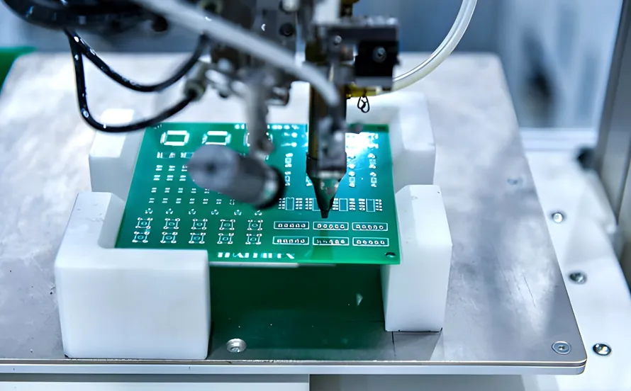
4. SMT Assembly
Surface-mount technology (SMT) is commonly used to assemble sensor PCBs because it supports compact components and high component density.
The typical process includes:
- Solder paste printing
- Component placement
- Reflow soldering
- Inspection
- Functional testing
Fine-pitch packages and miniature sensor components require accurate placement and tightly controlled reflow profiles.
5. Testing and Calibration
Testing is essential because a sensor PCB must not only operate electrically but also produce accurate measurements.
Depending on the application, manufacturers may perform:
- AOI
- X-ray inspection
- ICT
- Flying-probe testing
- Functional testing
- Sensor calibration
- Environmental testing
- Temperature cycling
- Burn-in testing
Calibration is particularly important when measurement accuracy is a critical product requirement.
Applications of Sensor PCBs

Sensor PCBs are used across almost every major electronics industry.
Automotive Applications
Automotive electronics rely heavily on sensors for monitoring and control.
Sensor PCBs are used in:
- Advanced driver assistance systems (ADAS)
- LiDAR systems
- Tire pressure monitoring systems (TPMS)
- Battery management systems
- Engine monitoring
- Temperature monitoring
- Vehicle stability systems
Electric vehicles are further increasing demand for high-performance sensor electronics because battery packs, power electronics, motors, and thermal management systems require extensive monitoring.
Medical Devices
Sensor PCBs are essential in many medical monitoring and diagnostic devices.
Applications include:
- Patient monitors
- Pulse oximeters
- Blood pressure monitors
- Temperature monitors
- Glucose monitoring systems
- Wearable medical devices
- Diagnostic instruments
These applications often require high accuracy, low noise, compact dimensions, and strict manufacturing controls.
Consumer Electronics
Smartphones, tablets, laptops, smartwatches, gaming devices, and smart home products contain numerous sensors.
Examples include:
- Accelerometers
- Gyroscopes
- Ambient light sensors
- Proximity sensors
- Temperature sensors
- Pressure sensors
The continuing trend toward smaller and more intelligent consumer products is driving the development of increasingly compact sensor PCBs.
Industrial Applications
Industrial sensor PCBs can monitor:
- Temperature
- Pressure
- Humidity
- Vibration
- Gas concentration
- Flow
- Smoke
- Equipment condition
They are widely used in industrial automation, predictive maintenance, process control, robotics, and machine monitoring.
Aerospace and Defense
Aerospace systems require reliable sensing under demanding environmental conditions.
Sensor PCBs can be used for:
- Engine monitoring
- Structural health monitoring
- Temperature measurement
- Pressure monitoring
- Vibration detection
- Environmental monitoring
- Navigation systems
These applications typically require high reliability, controlled manufacturing processes, and carefully selected materials.
Benefits of Sensor PCBs

Space Efficiency
Sensor PCBs integrate sensing elements, processing circuits, power management, and communication interfaces into a compact assembly.
This makes them particularly suitable for space-constrained products.
Improved Signal Quality
Integrating the sensor and signal-conditioning circuitry on a dedicated PCB can reduce interconnection length and minimize opportunities for noise pickup.
A carefully designed signal path can therefore improve measurement accuracy and repeatability.
High Reliability
A properly designed sensor PCB can integrate multiple functions into a single compact assembly, reducing the number of external interconnections and mechanical interfaces.
This can improve system reliability when combined with appropriate materials and manufacturing controls.
Better Connectivity
Built-in interfaces such as I²C, SPI, UART, CAN, and other communication technologies allow sensor data to be transferred efficiently to controllers and host systems.
Efficient Power Management
Power-management circuitry can optimize energy consumption, which is particularly valuable for battery-powered IoT devices, wearables, and remote monitoring systems.
Simplified Assembly
Integrating sensors and supporting electronics on one PCB can reduce wiring, simplify final assembly, and improve manufacturing consistency.
Challenges and Solutions in Sensor PCB Design
Miniaturization
Sensor electronics are becoming smaller while functionality continues to increase.
HDI PCB, microvias, fine-line technology, and mSAP can help designers achieve greater circuit density within a smaller footprint.
Environmental Exposure
Sensors may operate in environments containing:
- Moisture
- Dust
- Chemicals
- Salt spray
- High temperatures
- Mechanical vibration
Depending on the application, manufacturers may use conformal coatings, protective encapsulation, specialized housings, or environmentally resistant materials.
However, the protection method must not interfere with the sensing mechanism.
Cost Control
High-performance sensor PCBs may require specialized materials, fine-pitch components, advanced manufacturing processes, and calibration procedures.
To control costs, engineers should optimize:
- Layer count
- Material selection
- Component availability
- PCB dimensions
- Manufacturing tolerances
- Panel utilization
- Assembly process
Mechanical Fragility
Some miniature sensors and MEMS devices can be sensitive to mechanical stress, moisture, contamination, and thermal cycling.
Mechanical design, component placement, protective packaging, and controlled assembly processes are therefore important for long-term reliability.
Power Consumption
Battery-powered sensor nodes often need to operate for months or years without maintenance.
Low-power MCUs, sleep modes, efficient regulators, duty cycling, and low-power communication protocols can significantly extend operating life.
Cost Factors in Sensor PCB Manufacturing

Several factors determine the final cost of a sensor PCB.
Substrate Material
Standard FR-4 is generally economical, while polyimide, ceramic, high-frequency laminates, and other specialized materials can significantly increase material costs.
Layer Count
More PCB layers provide greater routing capacity, improved power distribution, and better electromagnetic shielding, but they also increase fabrication complexity and cost.
Manufacturing Tolerances
Sensor PCBs may require tighter dimensional, electrical, and assembly tolerances than standard circuit boards.
Higher precision can increase tooling, inspection, and production costs.
Component Selection
Specialized MEMS sensors, precision amplifiers, high-resolution ADCs, and low-noise components can contribute substantially to the total BOM cost.
Calibration and Testing
When a sensor PCB requires individual calibration or environmental testing, the additional testing time and equipment can increase manufacturing costs.
Future Trends in Sensor PCB Technology
The development of sensor PCBs is moving toward smaller dimensions, higher sensitivity, lower power consumption, greater intelligence, and improved integration.
Miniaturization Through HDI and mSAP
HDI and mSAP technology enable finer traces, smaller vias, and higher circuit density.
These technologies are particularly valuable for wearable devices, mobile electronics, medical equipment, and compact IoT nodes.
Flexible and Stretchable Electronics
Flexible substrates and stretchable electronic technologies are opening new possibilities for sensors that can conform to curved surfaces, textiles, and wearable products.
Future sensor systems may increasingly combine flexible circuits with embedded sensing elements and wireless communication.
Advanced Thermal Management
High-performance sensor systems will increasingly use advanced thermal-management technologies, including ceramic substrates, thermal vias, embedded heat-spreading structures, and specialized thermal materials.
These technologies can help maintain sensor accuracy in demanding temperature environments.
Edge Processing and AI
Another important trend is the integration of greater processing capability directly into sensor nodes.
Instead of continuously sending raw data to a remote server, sensor PCBs can increasingly process data locally using MCUs, DSPs, or AI-capable processors.
This can reduce:
- Communication bandwidth
- Latency
- Power consumption
- Cloud-processing requirements
It also enables smarter edge devices for predictive maintenance, autonomous systems, and industrial IoT applications.
Why Choose Kingda for Sensor PCB Manufacturing?
For demanding sensor PCB projects, selecting an experienced manufacturing partner is essential. Kingda can provide PCB fabrication, PCB assembly, engineering support, testing, and customized manufacturing solutions for different sensor applications.
When evaluating a sensor PCB manufacturer, consider:
- Manufacturing certifications and quality systems
- PCB fabrication capabilities
- SMT assembly capabilities
- Fine-pitch and HDI capabilities
- Component sourcing and supply-chain management
- AOI, X-ray, ICT, and functional testing
- Calibration capabilities where required
- Prototype and low-volume production support
- Mass-production capacity
- Engineering and DFM support
A reliable manufacturing partner should be capable of supporting the entire product-development cycle, from prototype validation to volume production.
How to Choose a Sensor PCB Manufacturer
Before selecting a supplier, evaluate the following factors:
Certifications and Quality Management
Verify that the manufacturer maintains appropriate quality-management certifications and follows relevant PCB manufacturing and assembly standards.
Testing Capabilities
Check whether the supplier can provide AOI, X-ray inspection, electrical testing, functional testing, environmental testing, and other requirements relevant to your application.
Prototype Services
A capable supplier should support rapid prototyping and engineering changes before mass production.
Component Procurement
Reliable component sourcing is particularly important for sensor PCBs because counterfeit or substituted components can directly affect measurement accuracy and system reliability.
Engineering Support
An experienced supplier should be able to review PCB layouts, materials, stackups, component placement, thermal requirements, signal integrity, and manufacturability before production.
Conclusion
A sensor PCB acts as a critical bridge between the physical world and the digital world. By integrating sensing elements with signal conditioning, data conversion, processing, power management, and communication circuits, sensor PCBs enable modern electronic systems to collect and interpret real-world information.
From automotive ADAS and medical monitoring equipment to industrial automation, aerospace systems, wearable electronics, and IoT devices, sensor PCBs are becoming increasingly important as products become smaller, smarter, and more connected.
Successful sensor PCB development requires more than simply placing a sensor on a circuit board. Engineers must carefully consider signal integrity, thermal management, component placement, material selection, power consumption, environmental protection, manufacturing tolerances, testing, and calibration.
As HDI, mSAP, flexible electronics, edge computing, and advanced sensor technologies continue to develop, sensor PCBs will become even more compact, intelligent, energy-efficient, and reliable.
For companies developing next-generation sensing products, working with an experienced sensor PCB manufacturer can help reduce design risk, improve manufacturing yield, accelerate prototyping, and establish a reliable path from engineering validation to mass production.