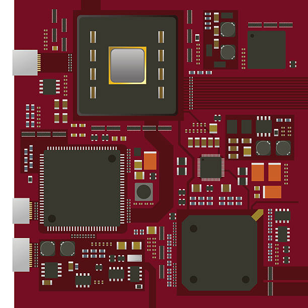
5G Base Station Antenna PCB Supplier: Process Checks
A 5G base station antenna board carries RF, power and control functions in one compact assembly. The supplier you choose decides whether that board holds its impedance, survives lamination and repeats the same result across lots. Most of that outcome is settled before the first panel is drilled. This review sets out the checks that separate a capable supplier from a confident quotation, and it explains what to verify at each stage of the build.
The board is not a simple circuit carrier. It is a transmission structure whose electrical behavior depends on copper geometry, dielectric thickness and layer registration. A small drift in any of these shifts phase, loss and return loss. Buyers should therefore treat the supplier’s process control as part of the electrical design, not as a separate purchasing question. The sections below follow the job from material choice to final test.
Material Choice Sets the Baseline
Material selection starts the process because the laminate fixes dielectric constant and loss. A low-loss laminate reduces attenuation, while a stable dielectric constant keeps impedance predictable across the panel. High-TG materials help where thermal cycling is part of the operating environment. PTFE systems and specialized high-frequency laminates enter when the application demands tighter RF performance. Each option carries different drilling, plating and lamination behavior, so the choice must match the factory’s proven process.
Ask the supplier how it qualifies incoming laminate. Certificates of analysis, batch traceability and stored samples all matter here. A material that quietly changes its resin content or copper roughness will shift insertion loss without any machine alarm. The buyer should confirm that the approved material is written into the process sheet and that substitutions require engineering approval. This single control prevents many field failures that later look like design problems.
Stackup and Layer Planning
The stackup defines the distance from each signal layer to its reference plane. That distance, together with trace width and copper thickness, sets characteristic impedance. Ground and power planes also shield sensitive RF traces from digital switching noise. A well-planned stackup separates antenna feed lines from control and power sections. It also reserves layers for thermal spreading where power density is high. The supplier should propose the stackup and explain each layer’s purpose.
Layer count follows routing density and isolation needs, not habit. Adding layers can improve shielding and space use, but it also adds lamination cycles and registration risk. The buyer should compare the proposed stackup against the electrical requirements and confirm the dielectric thickness at each interface. Board thickness, via structures and manufacturing tolerances belong in the same review. A stackup that ignores fabrication limits will fail at first article, so early agreement saves rework.
Controlled Impedance in Production
Impedance control connects the design target to the physical board. Trace width, copper thickness, dielectric constant and reference-plane distance all move the final value. Etching variation changes trace geometry, and lamination pressure changes dielectric thickness. The supplier must therefore hold these parameters inside a defined window and measure the result. Coupon testing on the panel gives evidence that the process stayed in control. Without that evidence, the impedance claim is only an intention.
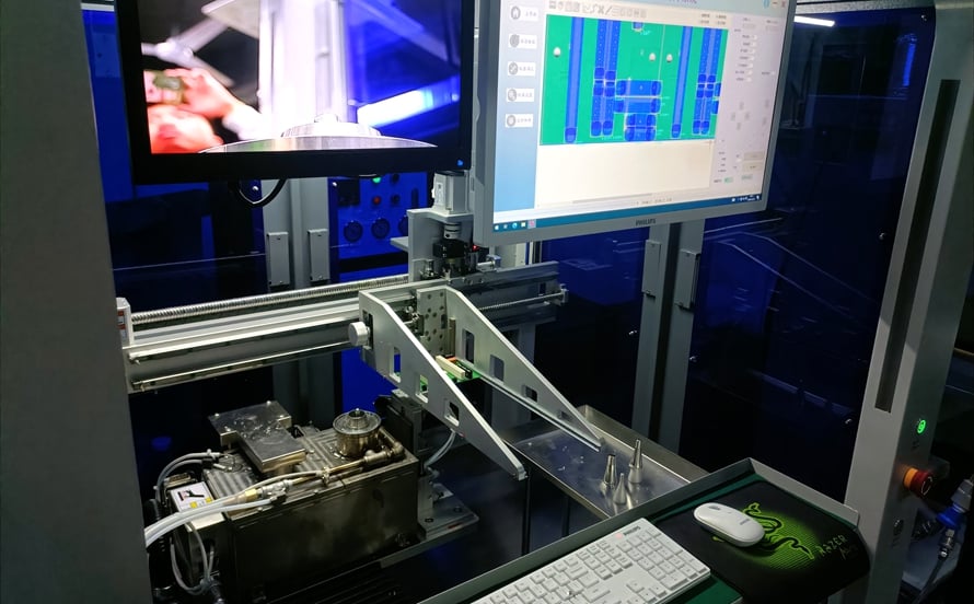
Ask how the factory handles a deviation. A capable supplier records the measured value, compares it with the agreed limit and raises a question before shipping. It should also explain how it compensates for copper thickness and resin flow during lamination. Buyers who review these details early avoid surprises at system test. The same discipline supports PCB design and layout, where trace geometry is fixed before fabrication begins.
Drilling and Via Reliability
Vias carry RF and power between layers, so their geometry affects both impedance and reliability. Drill accuracy, plating thickness and registration determine whether a via performs as designed. Microvias and blind structures raise routing density but demand tighter process control. Via-in-pad designs help with fine-pitch components, yet they need void-free filling and planarization. The supplier should show how it inspects plating thickness and via integrity. Cross-sectioning remains the clearest evidence of a sound barrel.
Thermal cycling exposes weak plating and poor resin adhesion. Buyers should ask which reliability tests the supplier applies and how it records the results. The answer should reference the actual stackup and material, not a generic claim. Where HDI is used, sequential lamination adds steps that each need inspection. A supplier that tracks layer registration after every cycle will catch drift before it becomes scrap.
Lamination and Surface Finish
Lamination bonds the stackup and fixes dielectric thickness across the panel. Pressure, temperature and resin flow must stay within a proven window. Poor control shows up as voids, resin starvation or thickness variation, and each of these changes impedance. The factory should record lamination parameters for every lot and keep them with the build record. Buyers can then trace a field issue back to a specific cycle. That traceability is a practical quality tool, not paperwork.
Surface finish protects exposed copper and affects solderability and RF loss. The choice depends on the assembly process, storage conditions and frequency range. The supplier should explain why a finish suits the application and how it controls thickness. Finish thickness variation can shift loss on high-frequency traces, so the process needs a defined limit. Buyers should confirm the finish in the drawing and check it at first article.
Inspection and Test Coverage
Inspection finds defects prior to shipment, yet its larger worth lies in the feedback it provides. When a defect appears, the engineer learns whether drilling, plating or lamination caused it. That loop between inspection and process control lowers defect rates over time. Electrical test confirms connectivity, while impedance coupons confirm transmission behavior. Functional checks add confidence where the board includes active devices. The test plan should match the board’s role in the system.
Ask for the records, not just the pass result. Batch records, coupon data and test reports show whether the process is genuinely controlled. A supplier that produces these documents on request usually keeps them honestly during production. Where the project includes assembled boards, PCBA testing extends the same discipline to the finished unit. Buyers should confirm who performs each test and where the results are stored.
Prototype to Production Transfer
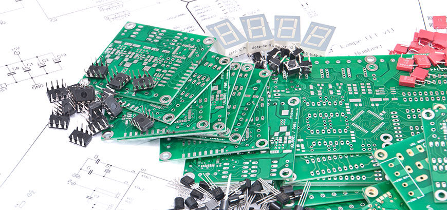
Most 5G hardware passes through several iterations before volume. The supplier should support requirement review, material choice, stackup development and DFM checks before tooling. Prototypes reveal pad geometry problems and process behavior while changes are still cheap. The transfer to production then depends on holding the same materials and parameters. A supplier that treats the prototype as a separate job often loses that continuity. Buyers should ask how the validated settings are carried forward.
Documentation is the bridge between stages. The process sheet, inspection plan and test limits should follow the design from first article to repeat order. When a parameter drifts, the record shows what changed and when. This is how a supplier keeps yield stable as volume grows. It also gives the buyer a fair basis for comparing quotations, because the scope of control is visible. Assembly scope can be added through PCB assembly when the project needs it.
Supplier Questions That Matter
When comparing boards, the price of each board is just one of several numbers to consider. Process controls, inspection equipment, material traceability and communication decide the real cost. A supplier that reviews files before production and reports risks honestly is usually cheaper over a program. Buyers should ask which parameters are recorded, who approves a material change and how deviations are reported. The answers reveal whether the quality system operates in practice. Vague replies are a warning sign.
Ask also about capacity and scheduling for the specific stackup. High-layer-count boards need lamination capacity and skilled operators. Quick-turn prototypes and volume orders compete for the same equipment, so the supplier should explain how it protects both. For projects that combine fabrication and assembly, turnkey PCB assembly can simplify the handoffs. Component sourcing is the other half of that decision, and component procurement deserves the same scrutiny as fabrication.
The practical takeaway is simple. Ask for the stackup, the impedance coupon data, the lamination record and the test report before you place the volume order. Confirm that the approved material and process settings are written down and that changes need your approval. A supplier that answers these questions with records is ready for 5G work. One that answers with assurances is not, however attractive the quotation looks.