Back Drilling PCB Supplier: Precision Technology for High-Speed Multilayer PCBs
In the manufacturing of high-layer-count and precision circuit boards, PCB back drilling is an important technology for improving high-speed signal transmission performance. By precisely removing the unnecessary portion of a plated through-hole, commonly known as a via stub, back drilling can reduce signal reflection, attenuation, resonance, and other electrical discontinuities.
For a reliable back drilling PCB supplier, the ability to integrate drilling accuracy, multilayer manufacturing, application-specific engineering, and responsive technical support is essential. These capabilities determine whether a manufacturer can consistently meet the electrical and mechanical requirements of advanced PCB applications.
Core Challenges of PCB Back Drilling: Precision and Process Coordination
The fundamental challenge of PCB back drilling is achieving a balance between precise material removal and protection of the active electrical connection.
Controlled-Depth Drilling Accuracy
Back drilling requires accurate control of drilling depth. The process must completely remove the unwanted via stub while avoiding damage to the copper layer or via structure that remains electrically functional.
A professional manufacturer needs precision CNC drilling equipment and reliable process-control systems to manage drilling depth and positional accuracy. For different PCB thicknesses, copper structures, dielectric materials, and layer configurations, drilling parameters must be adjusted accordingly.
Insufficient drilling can leave excessive via stubs that continue to affect high-speed signals. Excessive drilling, on the other hand, may damage an active copper connection or compromise the reliability of the board.
Therefore, controlled-depth drilling should be evaluated together with PCB stack-up, dielectric thickness, copper thickness, via geometry, and target connection layers.
Coordination With Multilayer PCB Manufacturing
Back drilling is not an isolated manufacturing operation. It is closely related to lamination, primary drilling, copper plating, inner-layer fabrication, registration, and final inspection.
For a complex multilayer PCB, layer-to-layer registration must be carefully controlled before the back-drilling operation. Stable registration provides the reference accuracy required for positioning the secondary drill.
The etching process also needs to maintain consistent conductor geometry. Variations in copper patterns or layer registration can affect drilling alignment and ultimately influence electrical performance.
Application-Specific Back Drilling Solutions
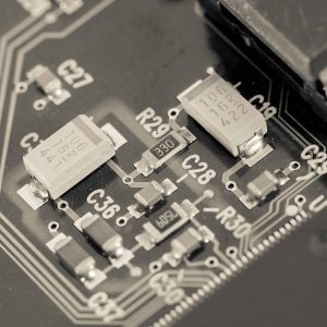
Different industries have different requirements for back-drilled PCBs. A capable back drilling PCB supplier should therefore provide application-specific engineering rather than relying on a single standard process.
High-Frequency and High-Speed Communication
In 5G infrastructure, networking equipment, data centers, servers, and other high-speed systems, unwanted via stubs can become increasingly significant as signal frequencies and edge rates increase.
Back drilling can shorten the electrical length of the via and reduce discontinuities in the signal path. When combined with appropriate high-frequency materials, stack-up design, impedance control, and optimized via structures, it can contribute to better signal integrity.
For advanced communication systems, high-speed PCB manufacturing should consider the entire signal path rather than treating back drilling as an independent process.
High-Frequency Multilayer Applications
High-frequency systems require careful control of dielectric properties, copper thickness, trace geometry, stack-up configuration, and impedance.
When back drilling is used in these designs, the drilling depth and remaining stub length should be determined according to the actual electrical requirements of the application.
High-Frequency Multilayer PCB Manufacturing
Industrial Control and Medical Electronics
Industrial control systems and medical electronics often require high reliability in addition to electrical performance.
For these applications, the quality of the back-drilled hole structure is important. The manufacturer should control burrs, resin debris, hole-wall condition, drilling depth, and layer integrity.
Additional electrical and dimensional inspections can help verify that the finished board meets the required reliability and performance specifications.
PCB Back Drilling and High-Speed Signal Integrity
The primary purpose of PCB back drilling is to reduce the electrical influence of unnecessary plated-through-hole sections.
A conventional through-hole can extend through the entire thickness of a board even when the signal only needs to connect a limited number of layers. The unused section becomes a via stub.
At higher frequencies, this stub can behave as an unwanted transmission-line section and contribute to:
- Signal reflection
- Impedance discontinuity
- Resonance
- Signal attenuation
- Crosstalk
- Electromagnetic interference
- Reduced signal integrity
By removing the unnecessary portion of the via, back drilling creates a shorter effective signal path.
However, back drilling should not be considered a standalone solution. Its effectiveness depends on the complete interconnection structure, including trace dimensions, dielectric properties, via geometry, reference planes, impedance requirements, and signal rise time.
The PCB Back Drilling Manufacturing Process
A reliable back drilling PCB supplier should integrate the back-drilling operation into the complete PCB fabrication workflow.
Step 1: Multilayer PCB Fabrication
Before back drilling begins, the basic multilayer PCB structure is manufactured.
Inner-layer circuits are fabricated and inspected. Core materials and prepreg are then stacked according to the designed layer structure and laminated together.
After lamination, primary drilling creates the through-holes required for electrical connections between layers.
Step 2: Through-Hole Plating
After drilling, the hole walls are treated and metallized to create conductive paths.
Electroless copper deposition and subsequent electroplating establish the required copper thickness on the hole walls.
At this stage, the through-hole generally extends through the full board thickness.
Step 3: Identify the Unused Via Section
The electrical connection requirements are analyzed to determine which portion of the through-hole is unnecessary.
For example, if a through-hole connects only the upper layers of a multilayer board, the remaining section below the target connection layer may become the unwanted via stub.
Step 4: Precision Back Drilling
A secondary drill with an appropriate diameter is used to remove the unwanted plated section.
The drilling depth is carefully controlled according to the PCB stack-up and target connection layer.
The objective is to remove as much of the unnecessary via structure as required while maintaining the integrity of the active electrical connection.
Step 5: Cleaning and Post-Processing
After drilling, copper particles, resin debris, and other contaminants must be removed.
Appropriate cleaning procedures help maintain hole quality and prevent debris from affecting subsequent manufacturing operations.
Depending on the board structure and manufacturing requirements, additional processes such as resin filling or copper capping may also be considered.
Step 6: Inspection and Verification
The finished board should be inspected to verify:
- Back-drill depth
- Remaining stub length
- Hole position
- Hole diameter
- Hole-wall condition
- Layer registration
- Copper integrity
- Overall board thickness
For demanding applications, cross-section analysis, electrical testing, impedance testing, and other engineering verification methods may also be appropriate.
Back Drilling Design Guidelines
Back drilling should be considered during PCB design rather than added after the layout has been completed.
Define the PCB Stack-Up First
The PCB stack-up determines the required back-drilling depth.
Designers should establish the layer structure, dielectric thickness, copper thickness, and target signal connections before defining the final drilling parameters.
Clearly Identify Back-Drilled Vias
Manufacturing data should clearly identify which vias require back drilling.
A separate drill file can be used to define back-drilled holes. File naming and documentation should clearly indicate the applicable drilling side and target layer range.
For example, manufacturing data may distinguish different structures by their drilling depth or designated layer connection.
The exact documentation method should always be confirmed with the selected PCB manufacturer before production.
Control the Remaining Stub
The objective of back drilling is to reduce the remaining via stub to an electrically acceptable length.
The appropriate remaining stub depends on signal frequency, rise time, via geometry, dielectric properties, board construction, and system-level signal-integrity requirements.
Designers should therefore avoid using a universal value without confirming the manufacturer’s process capability and the electrical requirements of the application.
Maintain Adequate Dielectric Clearance
Because back drilling is a controlled-depth machining operation, the distance between the bottom of the back-drilled hole and the adjacent functional layer must account for manufacturing tolerance.
Sufficient process margin helps prevent accidental damage to active copper structures.
Coordinate With the PCB Manufacturer
Different PCB manufacturers may have different drilling equipment, depth-control methods, minimum clearances, registration capabilities, and CAM requirements.
Early engineering review can help identify potential manufacturing problems before production begins.
Back Drilling Compared With Blind and Buried Vias
Back drilling, blind vias, and buried vias are different approaches to managing unnecessary via structures.
Back Drilling
Back drilling begins with a plated through-hole and removes the unused section after the primary hole has been plated.
Key advantages include:
- Reduced via stub length
- Improved high-speed signal performance
- Retention of a through-hole architecture
- Potentially reduced dependence on certain blind or buried via structures
Blind Vias
A blind via connects an external layer to one or more internal layers without extending through the entire PCB.
Blind vias are particularly useful in high-density designs where routing space is limited.
Buried Vias
A buried via connects internal layers without reaching either external surface.
This structure provides additional routing flexibility but generally requires more complex fabrication processes.
For advanced PCB designs, the selection between back drilling, blind vias, and buried vias should be based on signal integrity, routing density, layer structure, manufacturing capability, reliability, and cost.
HDI PCB Design and Manufacturing
How to Specify PCB Back Drilling in Manufacturing Data
Clear engineering documentation is essential when ordering PCB back drilling.
A typical manufacturing specification should include:
- Vias requiring back drilling
- Drilling side
- Starting layer
- Ending layer
- Drill diameter
- Finished hole diameter
- Back-drill depth
- Required remaining stub length
- PCB stack-up
- Dielectric thickness
- Resin filling requirements
- Copper capping requirements, when applicable
For complex projects, it is recommended that designers provide the complete fabrication data to the manufacturer for engineering review before production.
This approach can reduce misinterpretation of drill files and help ensure that the physical board matches the intended electrical design.
Important Considerations Before Using Back Drilling
1. Evaluate the Stack-Up
The layer structure directly determines the required drilling depth. The stack-up should therefore be finalized before back-drilled structures are defined.
2. Consider Drilling Tolerance
Back drilling is a depth-controlled process. Manufacturing tolerance must be considered when determining the drilling depth and dielectric clearance.
3. Minimize the Via Stub
The purpose is not simply to perform a secondary drilling operation. The objective is to reduce the unwanted via section to a length that is electrically acceptable for the application.
4. Review Manufacturing Capability
The selected back drilling PCB supplier should be able to review drilling depth, hole diameter, layer registration, stack-up, and related manufacturing constraints before production.
5. Consider Manufacturing Cost
Back drilling introduces an additional drilling operation and may increase manufacturing cost.
It should therefore be applied selectively to vias where the improvement in electrical performance justifies the additional manufacturing process.
Back Drilling for High-Speed PCB Applications
Back drilling is particularly valuable when high-speed signals pass through multilayer structures and conventional through-hole vias create excessive stubs.
Typical applications include:
- High-speed networking equipment
- Servers and data centers
- Telecommunications equipment
- High-performance computing systems
- Industrial communication equipment
- Advanced automotive electronics
- High-speed digital interfaces
- RF and mixed-signal systems
However, not every high-speed PCB automatically requires back drilling.
The appropriate solution depends on trace geometry, dielectric thickness, via dimensions, operating frequency, signal rise time, reference-plane configuration, target impedance, and the overall interconnection architecture.
A professional high-speed PCB manufacturing process should therefore evaluate back drilling together with stack-up design, controlled impedance, via optimization, and signal-integrity requirements.
Quality Control for PCB Back Drilling
Because PCB back drilling involves a precision secondary machining operation, quality control is essential.
A capable manufacturer should be able to verify:
- Drill depth
- Remaining stub length
- Hole diameter
- Layer registration
- Plated-hole integrity
- Resin filling
- Copper capping
- Board thickness
- Electrical performance
For complex high-speed boards, additional verification such as impedance testing, cross-section analysis, dimensional inspection, and electrical testing may be appropriate.
Engineering review should begin before fabrication so that potential issues can be identified during the design stage rather than after production.
Back Drilling vs. Standard Through-Hole Vias
The primary difference between a standard through-hole and a back-drilled via is the presence of an unnecessary plated section.
A standard through-hole remains plated through the complete PCB thickness.
A back-drilled via begins as a conventional plated through-hole, but the unused section is mechanically removed after plating.
This creates a shorter effective via structure and reduces the electrical influence of the via stub.
For high-speed and high-frequency applications, this approach can be an effective part of a broader signal-integrity strategy while allowing the PCB to retain a through-hole-based interconnection structure.
Choosing a Reliable Back Drilling PCB Supplier
Selecting the right back drilling PCB supplier requires more than evaluating whether a manufacturer can perform a secondary drilling operation.
A qualified supplier should demonstrate capabilities in:
- Precision controlled-depth drilling
- High-layer-count PCB fabrication
- High-frequency and high-speed PCB manufacturing
- Stack-up engineering
- Controlled impedance
- Via structure optimization
- Layer registration
- Electrical testing
- Engineering review
- Quality inspection
For demanding applications, manufacturing capability should be evaluated together with engineering experience and process consistency.
GOPCBA provides advanced PCB fabrication solutions for multilayer, HDI, high-frequency, high-speed, controlled-impedance, and other complex PCB structures. By combining engineering review with precision manufacturing and quality control, GOPCBA supports customers developing high-performance electronic products from prototype development through production.
Conclusion
PCB back drilling is an important manufacturing technology for reducing unnecessary via structures and improving signal transmission characteristics in advanced multilayer circuit boards.
By precisely removing the unwanted via stub, manufacturers can reduce potential signal reflection, resonance, attenuation, and impedance discontinuities. However, successful back drilling requires close coordination between PCB design, stack-up engineering, drilling parameters, layer registration, material selection, and quality inspection.
For high-speed communication, data center, RF, industrial, automotive, and other demanding applications, choosing an experienced back drilling PCB supplier can help ensure that the manufacturing process supports both electrical performance and long-term reliability.
GOPCBA provides advanced PCB manufacturing capabilities for complex multilayer, high-speed, high-frequency, HDI, and impedance-controlled applications, helping customers develop reliable PCB solutions for demanding electronic systems.