Electronic devices continue to become more powerful and compact, and this increasing complexity is particularly apparent to PCB designers during the routing stage. Modern processors, SoCs, FPGAs, BGAs, memory devices, and high-speed interfaces have increasingly dense pin layouts. As a result, designers must maximize available routing channels while maintaining the required electrical clearance, isolation, impedance, and signal-integrity requirements of critical nets.
This is a continuous balancing act in every new PCB design. The objective may be to significantly reduce board size while maintaining or improving electrical performance through advanced HDI PCB technology.
HDI is not limited to AI inference servers or high-performance computing platforms. Any electronic product that needs more functionality in a smaller footprint can benefit from increased routing density.
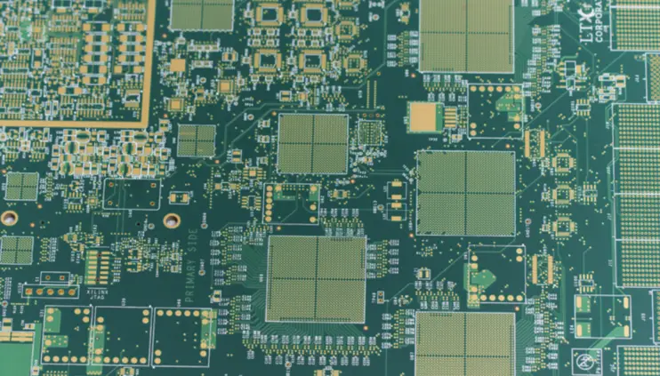
HDI PCB technology allows designers to accommodate more circuitry within fewer or more efficiently utilized PCB layers. Shorter traces can also reduce signal travel distance, while microvias and advanced interconnect structures can eliminate some of the space limitations created by conventional through-hole vias.
One important advantage of High Density Interconnect technology is its ability to localize layer-to-layer connections. Conventional through-hole pads and vias can occupy space across multiple PCB layers, potentially blocking routing channels. HDI microvias, by comparison, can connect only the layers required by a specific circuit.
This approach can reduce unnecessary via stubs, improve routing flexibility, and create additional space for high-density circuitry.
However, HDI is not a universal solution. It introduces more sophisticated manufacturing requirements and must be carefully balanced against cost, reliability, electrical performance, and production volume.
Key Considerations for HDI PCB Design
A successful HDI PCB design requires more than simply reducing trace width and via diameter. Engineers should consider the complete electrical and manufacturing architecture of the board.
Key areas include:
- Power and ground planning around SoCs and high-performance devices
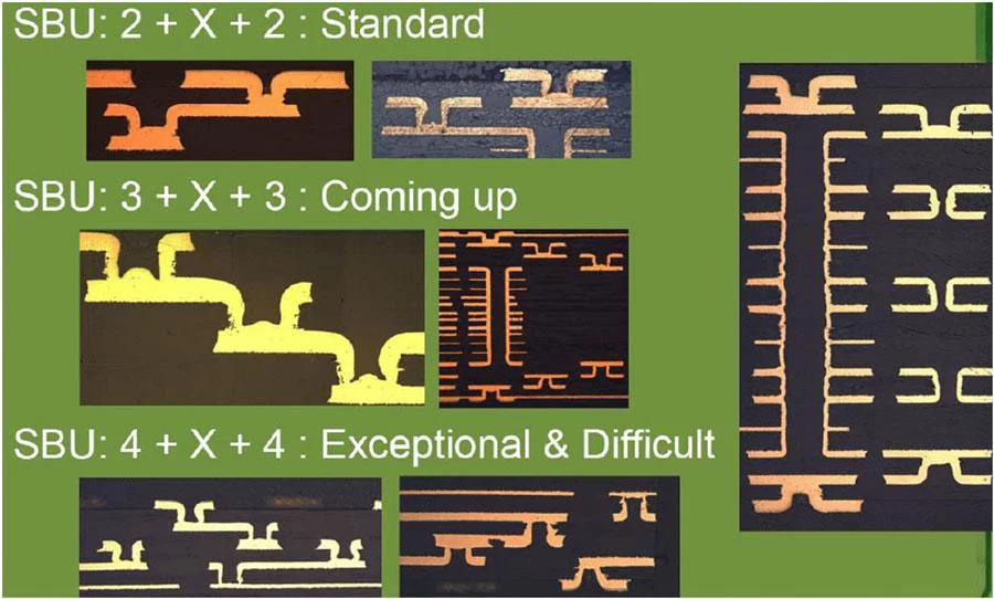
- Staggered vs. stacked microvias
- Localized routing and constraint regions
- Signal integrity and controlled impedance
- Thermal management
- ECAD-based constraint management
- BGA escape routing
- PCB stack-up optimization
- DFM and manufacturing capability
- Prototype-to-production scalability
Kingda can support these requirements through integrated PCB manufacturing and PCBA assembly, allowing HDI projects to be evaluated from both the design and manufacturing perspectives.
The Definition of HDI and Why It Is Necessary
High Density Interconnect (HDI) is a broad category of PCB technology that uses finer circuit geometries and advanced interconnection structures to achieve greater wiring density.
There is no single dimensional value that defines every HDI PCB because manufacturing standards and capabilities vary. However, fine-line routing, laser-drilled microvias, blind vias, buried vias, sequential lamination, and fine-pitch BGA routing are common characteristics of HDI technology.
The microvia is one of the most important technologies behind HDI.
Typical microvias are significantly smaller than conventional mechanically drilled vias. Their actual dimensions depend on the PCB fabricator’s process capabilities, material system, layer thickness, aspect ratio, and reliability requirements.
For example, microvia hole diameter, capture-pad size, and maximum depth must be evaluated together. A smaller hole does not automatically result in a better PCB. The selected geometry must remain compatible with laser drilling, copper plating, lamination, and long-term reliability requirements.
For this reason, DFM (Design for Manufacturing) should be considered at the beginning of the PCB design process.
With Kingda’s PCB engineering and manufacturing capabilities, designers can evaluate the feasibility of HDI structures before committing to a production design. This helps align the PCB layout with practical manufacturing requirements.
Thermal Management Is Always a Concern for HDI Designs
Thermal management becomes increasingly important as PCB designs become more compact.
High-density boards typically contain processors, memory devices, power-management components, communication ICs, and other heat-generating components within a limited area. As component density increases, managing junction temperatures becomes one of the major limitations to further miniaturization.
Even with extensive signal routing, the thermal paths through the PCB must remain robust.
A successful thermal strategy should consider:
- Thermal vias
- Copper planes
- Heat-spreading layers
- Component placement
- PCB material
- Heat sinks
- Airflow
- Liquid cooling
- System-level thermal interfaces
For lower-power electronics such as laptops and portable devices, forced-air cooling may be sufficient. For higher-power applications such as AI infrastructure, networking equipment, advanced computing systems, and high-performance industrial electronics, more sophisticated cooling technologies may be required.
This means thermal design should not be treated as a final-stage activity. It should be considered during PCB placement, stack-up planning, and routing.
Power Delivery Network Design for HDI PCBs
A reliable Power Delivery Network (PDN) should begin with a well-defined power tree for the entire board.
Power and ground planning should follow major component placement as early as possible. This is especially important around SoCs, FPGAs, GPUs, processors, and other high-current or high-speed devices.
The power architecture should ideally be incorporated into the schematic early in the development cycle. This gives the PCB designer a better understanding of voltage domains, current requirements, power sequencing, and decoupling requirements.
Using two or more adjacent PCB layers for power distribution can provide a wider effective current path while potentially freeing routing space on layers that would otherwise be heavily occupied by power copper.
A well-designed PDN can improve:
- Power integrity
- Voltage stability
- Current distribution
- Return-current paths
- EMI performance
- High-speed signal performance
- PCB routing efficiency
Kingda can support customers developing complex multilayer and HDI PCBs where controlled impedance, power distribution, and thermal considerations must be evaluated together.
Ground Vias Are an Essential Starting Point
Ground vias provide both electrical and thermal benefits, making them an important component of HDI PCB design.
For high-speed signals, a properly designed ground-return path helps maintain signal integrity. When a high-speed trace transitions between layers, its return current needs an appropriate reference path.
If the reference plane changes or the return path is interrupted, current may be forced to take a longer route. This can increase loop area and potentially contribute to EMI, crosstalk, and signal distortion.
HDI structures can provide greater flexibility when designing return paths.
However, excessive ground vias can also reduce routing space. The objective is therefore not to maximize the number of vias, but to place them where they provide the greatest electrical and thermal benefit.
Staggered or Stacked Microvias: Pros and Cons
When it comes to mass production, PCB cost matters. The bare PCB can represent a significant portion of the overall bill of materials, particularly for complex HDI designs.
The choice between staggered microvias and stacked microvias therefore requires careful consideration.
Staggered Microvias
In a staggered microvia structure, adjacent microvias are offset from one another rather than vertically aligned.
The main advantage is that the structure can provide greater manufacturing flexibility in certain designs.
The disadvantage is that staggered structures generally consume more horizontal PCB space.
This additional space can become a significant issue when routing fine-pitch BGA devices.
Stacked Microvias
Stacked microvias are vertically aligned across multiple layers and provide a more compact interconnection structure.
Their major advantages include:
- Higher routing density
- Better utilization of PCB space
- Improved fine-pitch BGA escape routing
- More direct vertical connections
- Greater flexibility for advanced HDI stack-ups
The trade-off is manufacturing complexity.
Stacked microvias may require additional process controls, including more demanding laser drilling, sequential lamination, copper filling, and registration processes.
For this reason, the most efficient electrical structure is not always the most economical manufacturing structure.
Kingda can evaluate the required microvia structure, stack-up, layer count, material system, and manufacturing requirements to help determine whether stacked or staggered microvias are appropriate for a specific application.
Advanced Any-Layer HDI Structures
The most demanding high-density devices may require HDI stack-ups with minimal dependence on conventional core vias.
Any-layer HDI provides designers with greater flexibility by allowing microvia connections to be distributed across the PCB stack-up.
This approach can be particularly useful for:
- Fine-pitch BGAs
- High-pin-count processors
- FPGAs
- GPUs
- Advanced memory interfaces
- High-speed communication devices
Any-layer technology extends the high-density interconnect concept across the PCB, providing routing flexibility similar to advanced package-substrate technology.
However, the manufacturing process is more demanding.
Before selecting an any-layer structure, designers should confirm:
- Microvia diameter
- Capture-pad size
- Aspect ratio
- Laser drilling capability
- Copper filling process
- Layer registration
- Sequential lamination
- Copper thickness
- Material compatibility
- Controlled impedance capability
- Production yield
Kingda’s manufacturing engineering team can work with customers to evaluate the relationship between the required HDI structure and the intended production process.
Use ECAD Tools to Create a Digital Design Model
When dealing with high-speed buses, HDI routing becomes a multidimensional design problem.
Timing requirements mean that signal lengths often need to be matched to clocks, strobes, or other reference nets. Establishing electrical constraints for relative propagation delay allows ECAD software to provide interactive feedback during routing.
Designers can use delay-tuning functions to meet timing budgets while minimizing unnecessary meandering.
A properly configured ECAD environment can manage:
- Length matching
- Propagation delay
- Differential pairs
- Impedance
- Net classes
- Net groups
- Byte lanes
- Routing layers
- Clearance
- Via restrictions
Modeling bus routing before detailed routing begins can significantly improve design efficiency.
For example, assigning byte lanes within the constraint manager allows engineers to visualize related nets and identify potential routing conflicts before they become major layout problems.
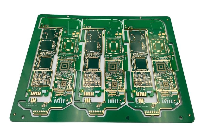
Net Groups and Floorplanning Improve Routing
Establishing net groups provides immediate insight into congested regions of the PCB layout.
Related signals can be grouped according to their electrical or functional role, such as:
- DDR memory
- PCIe
- USB
- Ethernet
- SerDes
- Clock signals
- Differential pairs
- Power networks
A bus that passes through several devices can also benefit from flow planning.
By defining preferred routing layers in advance, designers can reserve critical routing resources and avoid unnecessary layer changes.
This leads to a more systematic PCB design process:
Component Placement → Power Planning → Floorplanning → Constraint Definition → BGA Escape Routing → High-Speed Routing → Verification
This approach is particularly valuable for HDI boards because routing congestion can become difficult to resolve once the available space has been consumed.
Constraint Regions Decouple Dense Areas from the Rest of the Board
Constraint regions are one of the most effective methods for managing context-sensitive PCB design rules.
Not every section of a PCB requires the same trace width, spacing, impedance, or routing density.
For example, a fine-pitch BGA may require extremely tight routing geometry, while a low-speed control section of the same PCB can use much more conventional design rules.
Applying the strictest rules to the entire board can unnecessarily increase manufacturing cost and design complexity.
Instead, designers can create localized rules for specific areas.
Typical regions may include:
BGA Escape Region
Fine-line routing and tighter spacing rules can be applied only around the BGA.
High-Speed Interface Region
Controlled impedance, differential-pair, and length-matching rules can be applied to PCIe, USB, Ethernet, or SerDes interfaces.
Connector Region
Pin-to-trace and pin-to-shape clearance rules can be customized according to connector geometry.
Standard PCB Region
The majority of the board can continue using standard manufacturing rules.
This approach provides the required performance without imposing expensive HDI manufacturing requirements on areas that do not need them.
Neck-Down Routing for High-Density Areas
The next level of localized control involves neck-down routing.
Traces can use a standard width across most of the PCB and temporarily reduce in width when entering a high-density area.
This can provide additional routing channels around BGA devices and connectors.
For differential pairs and controlled-impedance signals, however, neck-down sections should generally be kept as short as practical and verified against the required impedance profile.
In some cases, it is more effective to invoke neck-down routing only when necessary rather than applying a permanent regional constraint.
This provides the designer with greater control while avoiding unnecessary restrictions elsewhere on the PCB.
Surface-Mount Devices Require Localized Design Rules
Surface-mount devices (SMDs) also benefit from more flexible regional constraints.
Rather than applying one rule to every PCB layer, designers can specify different requirements for:
- Outer layers
- Signal layers
- Plane layers
- Power layers
- High-speed routing layers
This provides enough context for design rules to solve specific routing problems without unnecessarily restricting the entire PCB.
The objective is not to make every part of the PCB follow the most aggressive design rules.
The objective is to apply the right rule to the right region.
Kingda: HDI PCB and PCBA Manufacturing Support
A successful HDI design must ultimately be manufacturable.
The PCB designer may be able to complete a highly complex layout in an ECAD system, but the design still needs to be compatible with the PCB manufacturer’s actual fabrication and assembly capabilities.
Kingda provides integrated PCB manufacturing and PCBA assembly services, supporting customers from PCB prototype and fabrication through component sourcing, SMT, DIP/THT assembly, inspection, testing, and final product assembly.
For complex HDI projects, Kingda’s capabilities can support requirements including:
- HDI PCB manufacturing
- Multilayer PCB fabrication
- Microvia PCB
- Blind and buried vias
- Via-in-pad
- Fine-line PCB
- Controlled impedance PCB
- High-speed PCB
- High-frequency PCB
- Flexible PCB
- Rigid-flex PCB
- BGA assembly
- SMT assembly
- DIP/THT assembly
- SPI inspection
- AOI inspection
- X-ray inspection
- ICT and functional testing
- DFM/DFA engineering support
This integrated manufacturing model allows PCB requirements to be evaluated from both the design and production perspectives.
Kingda’s DFM Advantage for HDI PCB Projects
HDI designs require close attention to manufacturability.
Kingda can provide DFM/DFA engineering support to help review PCB layouts, manufacturing files, component requirements, stack-up structures, spacing, and assembly considerations before production.
This can help identify potential problems such as:
- Excessively aggressive trace geometry
- Difficult microvia structures
- Insufficient clearances
- Unnecessary manufacturing complexity
- Component availability issues
- BGA assembly risks
- Test-access limitations
- Potential production-yield concerns
Early DFM review can reduce redesign cycles and help engineers move more efficiently from prototype to production.
Kingda Supports Prototype to Mass Production
HDI products often require several development stages.
A typical process may include:
PCB Design → DFM Review → PCB Prototype → PCBA Prototype → Testing → Design Optimization → Pilot Production → Mass Production
Kingda supports this progression through integrated PCB fabrication and PCBA manufacturing.
Working with one manufacturing partner from prototype through production can simplify communication and help maintain greater consistency in materials, fabrication processes, component sourcing, assembly methods, inspection, and testing.
For customers developing complex electronic products, this can make the transition from engineering validation to production more efficient.
How to Achieve a Better HDI PCB Design
A successful HDI PCB is not simply the board with the smallest trace width or smallest via diameter.
The best design balances:
- Component placement
- BGA escape routing
- Power integrity
- Signal integrity
- Controlled impedance
- Ground-return paths
- Thermal management
- Microvia structure
- PCB stack-up
- Regional constraints
- Manufacturing cost
- Production yield
- Long-term reliability
The real value of HDI technology lies in its ability to make more efficient use of the available PCB space while maintaining electrical and mechanical performance.
By combining microvias, fine-line routing, optimized stack-ups, controlled impedance, ECAD constraints, thermal planning, and DFM analysis, engineers can solve routing challenges that would otherwise require larger boards or additional PCB layers.
At the same time, HDI design should always be developed with manufacturing in mind.
Selecting the right PCB manufacturer early in the design process allows engineers to verify whether the chosen microvia structure, stack-up, trace geometry, materials, impedance requirements, and tolerances are realistic for production.
With integrated PCB fabrication, HDI PCB manufacturing, component sourcing, SMT/DIP assembly, inspection, testing, and final assembly, Kingda provides a one-stop manufacturing solution for complex electronic products.
From PCB prototype to mass production, Kingda can help customers transform high-density PCB designs into reliable, production-ready electronic assemblies.
Conclusion
As electronic products continue to become smaller, faster, and more powerful, HDI PCB technology will play an increasingly important role in advanced electronic design.
The challenge is not simply increasing routing density. Engineers must simultaneously manage signal integrity, power integrity, thermal performance, manufacturing complexity, cost, and reliability.
From power and ground planning to stacked and staggered microvias, from ECAD constraint management to localized routing rules, every design decision affects the final performance and manufacturability of the PCB.
A successful HDI PCB therefore requires close cooperation between PCB designers, electrical engineers, manufacturing engineers, and the PCB manufacturer.
With its integrated HDI PCB manufacturing, PCB fabrication, PCBA assembly, component sourcing, DFM/DFA support, inspection, testing, and final assembly capabilities, Kingda can support complex electronic projects from initial PCB development through production.
For companies looking for a reliable HDI PCB manufacturer and PCBA partner, Kingda provides an integrated manufacturing solution designed to support high-density, high-speed, and complex electronic products from prototype to volume production.