PCB Layout Design Services for High-Speed and HDI PCBs
PCB layout design is the process of transforming an electrical schematic into a physical printed circuit board (PCB) layout that meets the required electrical, mechanical, manufacturing, and performance requirements. A well-designed PCB layout not only ensures reliable electrical connections but can also improve signal integrity, reduce manufacturing costs, enhance PCBA performance, and shorten product development cycles.
PCB layout is an essential part of hardware development. Even when the circuit schematic is technically sound, the physical layout can have a significant impact on signal quality, electromagnetic compatibility (EMC), power integrity, thermal performance, manufacturability, and overall product reliability.
For complex electronic products, PCB layout requires much more than simply placing components and routing traces. High-speed signals, differential pairs, impedance-controlled traces, multilayer stack-ups, power distribution, grounding, EMI/EMC, thermal considerations, and manufacturing constraints must all be considered during the design process.

GOPCBA provides professional PCB design and layout services for standard, multilayer, high-speed, HDI, flexible, rigid-flex, and mixed-signal circuit boards. Our engineers work from customer schematics, netlists, BOMs, mechanical drawings, and design requirements to develop practical PCB layouts that are optimized for electrical performance and manufacturing.
Explore GOPCBA PCB Design & Layout Services
What Is PCB Layout Design?
PCB layout design refers to arranging electronic components and routing electrical connections on a printed circuit board according to the circuit schematic and engineering requirements.
The schematic defines what the circuit does, while the PCB layout determines how the circuit is physically implemented.
A professional PCB layout should achieve several objectives:
- Ensure all electrical nets are correctly connected.
- Maintain signal integrity for high-speed and sensitive signals.
- Control impedance where required.
- Minimize electromagnetic interference and crosstalk.
- Provide reliable power and ground distribution.
- Maintain appropriate thermal performance.
- Meet mechanical and enclosure requirements.
- Follow PCB manufacturing and assembly requirements.
- Reduce unnecessary production costs.
- Improve overall product reliability.
For digital circuits, layout quality is closely related to noise margins, timing, signal integrity, and electromagnetic compatibility. For analog circuits, minimizing noise, interference, parasitic effects, and unwanted coupling is particularly important.
Therefore, PCB layout is not simply a matter of connecting components. It is an engineering process that translates electrical requirements into a manufacturable physical design.
How to Create a PCB Layout From a Schematic
Creating a PCB layout from a schematic requires a structured engineering process. The exact workflow varies according to board complexity, but the following steps provide a practical foundation.
1. Review the Schematic and Design Requirements
Before starting PCB placement, engineers should carefully review the schematic, BOM, netlist, mechanical requirements, and design specifications.
Important information may include:
- Component packages
- Critical signal definitions
- Differential pairs
- High-speed interfaces
- Power requirements
- Impedance requirements
- PCB layer requirements
- Stack-up specifications
- Mechanical constraints
- Connector positions
- Thermal requirements
- EMC requirements
- Manufacturing limitations
A correct netlist is essential because it defines the electrical relationships between components.
2. Define the PCB Outline and Mechanical Constraints
The PCB outline should be established according to the mechanical design.
Engineers should define:
- Board dimensions
- Mounting holes
- Connector locations
- Keep-out areas
- Component height restrictions
- Mechanical interfaces
- Heat dissipation areas
- Board-to-board connection areas
The mechanical structure should be considered before detailed component placement begins.
3. Plan the PCB Stack-Up
For multilayer PCBs, layer planning is one of the most important parts of the layout process.
A typical stack-up may include:
- Signal layers
- Ground planes
- Power planes
- Additional routing layers
High-speed signals should preferably be routed adjacent to a continuous reference plane to provide a controlled return path.
Important signal groups such as DDR, PCIe, USB, high-speed Ethernet, RF signals, and differential pairs may require dedicated routing strategies.
The stack-up should also consider:
- Controlled impedance
- Dielectric thickness
- Copper thickness
- Signal return paths
- Crosstalk
- Power integrity
- Manufacturing capability
For advanced PCB layouts, stack-up design and impedance calculation should be completed before critical routing begins. GOPCBA’s PCB design service includes PCB stack-up design, impedance calculation, board design, reverse engineering, and EMC inspection.
4. Place Components According to Functional Blocks
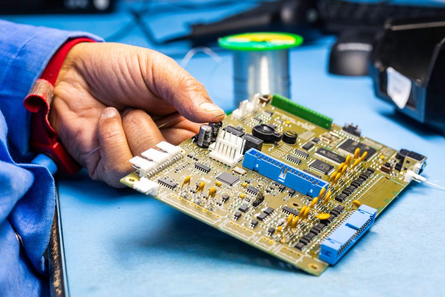
Component placement should follow the functional architecture of the circuit.
A common approach is to divide the PCB into functional blocks such as:
- Main processor
- Memory
- Power supply
- Communication interfaces
- Analog circuits
- Digital circuits
- RF circuits
- Protection circuits
- Sensors
- Connectors
The main MCU or processor may be positioned according to the overall architecture, while interface circuits should generally be located close to their corresponding connectors.
For example, USB, Ethernet, VGA, and other external interfaces should be placed near their physical connectors. ESD protection and filtering components should also be positioned appropriately within the signal path.
The general principle is to maintain short and logical signal paths while minimizing unnecessary coupling.
Key PCB Component Placement Principles
Keep Functional Blocks Clearly Defined
A good PCB layout should allow engineers to understand the functional architecture simply by looking at the board.
Components belonging to the same circuit should normally be placed together, while unrelated circuits should be physically separated where appropriate.
Separate High-Speed and Low-Speed Circuits
High-speed circuits can generate significant electromagnetic noise and should be separated from sensitive low-speed or analog circuits when possible.
Separate Analog and Digital Circuits
Analog circuits are often more sensitive to noise. Digital switching signals should therefore be routed and placed carefully to avoid unwanted coupling into analog sections.
Separate Noise Sources From Sensitive Circuits
Typical noise sources include:
- Switching power supplies
- High-speed processors
- Clock circuits
- High-current switching devices
- High-speed interfaces
Sensitive circuits may include:
- ADC/DAC circuits
- Analog amplifiers
- RF circuits
- Sensors
- Precision measurement circuits
Physical separation and appropriate grounding can significantly reduce unwanted interference.
PCB Power Distribution and Grounding
Power distribution is a critical part of PCB layout.
The main power supply circuit should generally be positioned close to the power entry point. Local power regulators or power modules can then be placed near the circuits they supply.
Power traces should provide sufficient current-carrying capacity. High-current paths should normally be short and wide to reduce voltage drop and unnecessary impedance.
From an EMC perspective, the complete current-return path is particularly important.
A large current loop can behave like an antenna and increase electromagnetic radiation. Therefore, the power loop should be kept as small as practical.
Proper grounding and continuous reference planes are also important for high-speed PCB design.
High-Speed PCB Layout
High-speed PCB layout requires careful control of electrical characteristics that are often less important in low-speed designs.
Important considerations include:
- Controlled impedance
- Signal propagation delay
- Differential pair routing
- Trace length matching
- Timing
- Crosstalk
- Reflections
- Return paths
- Via transitions
- Reference plane continuity
- Termination strategies
High-speed interfaces such as PCIe, SATA, SAS, SFP, XAUI, USB, and high-speed Ethernet require carefully controlled routing.
GOPCBA’s PCB design capabilities support complex high-frequency, high-density, high-speed, mixed-signal, multilayer, HDI, impedance-controlled, blind-via, and buried-via designs. The published capability includes support for signals up to 56G-PAM4.
Differential Pair and Length Matching
Differential pairs should be routed according to the electrical requirements of the interface.
Important parameters include:
- Differential impedance
- Pair spacing
- Trace width
- Length matching
- Skew
- Reference plane
- Via transitions
Signals that require timing matching should be routed according to the specified tolerance rather than simply making every trace the same length.
For high-speed buses, timing differences can directly affect system performance.
Signal Integrity and Power Integrity Analysis
Simulation and analysis can help identify potential problems before prototype manufacturing.
Signal Integrity Analysis
Signal integrity analysis may include:
- Impedance analysis
- Reflection analysis
- Crosstalk analysis
- Timing analysis
- Eye diagram evaluation
- Differential signal analysis
- Topology analysis
- Termination strategy
Power Integrity Analysis
Power integrity analysis focuses on:
- Power distribution
- Decoupling strategy
- Voltage stability
- Current distribution
- Power plane design
- Grounding
- PDN behavior
Early analysis helps reduce the risk of redesign, prototype failure, and unexpected signal problems.
EMC and EMI Considerations
EMC should be considered throughout PCB layout rather than treated as a final-stage inspection item.
Good PCB layout practices include:
- Keeping high-speed traces short.
- Maintaining continuous reference planes.
- Minimizing current-loop areas.
- Separating noise sources from sensitive circuits.
- Positioning filtering components correctly.
- Providing appropriate grounding.
- Controlling return paths.
- Avoiding unnecessary trace crossings.
- Reducing coupling between sensitive circuits.
A layout that considers EMC from the beginning can reduce the risk of electromagnetic interference during later testing.
PCB Layout for Different Board Technologies
Professional PCB layout services may cover a wide range of PCB technologies.
Single-Layer and Double-Layer PCB
Simple PCB designs may use single-layer or double-layer structures. These boards are suitable for relatively straightforward circuits and cost-sensitive products.
Multilayer PCB
Multilayer PCBs provide additional routing capacity and dedicated power and ground planes.
They are widely used for:
- Computers
- Industrial electronics
- Communication equipment
- Medical devices
- Automotive electronics
- High-density electronic products
HDI PCB
HDI PCB design uses technologies such as microvias, blind vias, buried vias, and fine-pitch routing to achieve higher component density.
HDI layout requires careful coordination between:
- Layer stack-up
- Via structure
- BGA escape routing
- Impedance
- Manufacturing process
- Signal integrity
Flexible and Rigid-Flex PCB
Flexible and rigid-flex PCBs combine electrical functionality with mechanical flexibility.
Their layout must consider:
- Bend areas
- Bend radius
- Copper routing
- Stiffener requirements
- Mechanical stress
- Connector transitions
PCB Layout Design Workflow
A structured workflow helps improve design quality and development efficiency.
Step 1: Submit Project Documents
Typical design inputs include:
- Schematic
- Netlist
- BOM
- Mechanical drawing
- DXF file
- Design guidelines
- Stack-up requirements
- Impedance requirements
- Critical signal requirements
Step 2: Engineering Review and Quotation
The engineering team reviews the project requirements, board complexity, component count, signal requirements, and manufacturing constraints before confirming the design scope.
Step 3: Preliminary Component Placement
Engineers create the initial placement according to the schematic, mechanical structure, functional blocks, and critical signal requirements.
Step 4: Customer Layout Review
The preliminary layout can be reviewed before detailed routing.
Items for confirmation may include:
- Board outline
- Component placement
- Stack-up
- Connector positions
- Impedance requirements
- Routing strategy
- Mechanical clearance
Step 5: PCB Routing
Engineers then complete the detailed routing according to the design rules.
Critical signals are generally routed first, followed by other signal groups.
Step 6: DFM, EMC and Design Verification
The completed layout should be checked for:
- Design rule violations
- Manufacturing limitations
- Signal integrity
- Power integrity
- EMC
- Clearance
- Component placement
- Routing
- Impedance
- Thermal considerations
Step 7: Final Data Output
After the layout has been reviewed and approved, the required production files can be generated, including:
- PCB source files
- Gerber files
- Drill files
- Assembly files
- BOM
- Pick-and-place files
- Mechanical files
- Manufacturing documentation
PCB Layout Software
Professional PCB engineers may use a range of industry-standard PCB design tools, including:
- Cadence Allegro
- Altium Designer
- PADS
- Eagle
- Protel
GOPCBA supports popular PCB design platforms including Altium Designer, Cadence, Allegro, Eagle, and PADS.
PCB Layout for Industrial Electronics
Industrial electronics often require high reliability, stable operation, and careful thermal and EMC design.
PCB layout for industrial applications may involve:
- Industrial computers
- PLC systems
- DCS and FCS systems
- CNC equipment
- ARM-based controllers
- x86-based systems
- Power electronics
- Industrial communication systems
GOPCBA provides PCB manufacturing and assembly solutions for industrial control applications, including PCB layout, fabrication, component sourcing, and assembly.
PCB Layout for Communication Equipment
Communication equipment places particularly high demands on signal integrity.
Typical applications include:
- High-speed communication boards
- Optical communication equipment
- SFP interfaces
- High-speed connectors
- CPCI systems
- ATCA systems
- VME systems
- PXI systems
High-speed signal rates may require strict control of:
- Crosstalk
- Reflection
- Insertion loss
- Return loss
- Impedance
- Timing
Careful routing and stack-up design are essential for maintaining signal quality.
PCB Layout for Consumer Electronics
Consumer electronics often require high-density layouts with compact mechanical dimensions.
Typical requirements include:
- HDI design
- Fine-pitch BGA routing
- RF signal routing
- High-speed interfaces
- Compact component placement
- EMI/EMC control
- ESD protection
Applications may include smartphones, digital cameras, wireless products, IoT devices, and other compact electronics.
PCB Layout for Security and Surveillance Equipment
Security and surveillance products require reliable processing of video, audio, network, and control signals.
PCB layout considerations may include:
- High-speed video signals
- Network interfaces
- Processor placement
- Memory routing
- EMI control
- Thermal management
- ESD protection
High-speed video and audio circuits should be carefully separated from potential noise sources.
PCB Layout for Automotive Electronics
Automotive electronic products require careful consideration of electrical reliability, mechanical constraints, EMI, and thermal performance.
Typical applications include:
- Vehicle computers
- Dash cameras
- Rear-view systems
- Single-camera systems
- Dual-camera systems
- Dual-1080p video systems
- Automotive peripheral electronics
Automotive PCB layouts should be developed according to the specific electrical and environmental requirements of the application.
PCB Reverse Engineering
PCB reverse engineering can be used when original PCB design files, schematics, or documentation are unavailable.
A reverse-engineering project may involve:
- PCB inspection
- Layer identification
- Component identification
- Netlist reconstruction
- Schematic recreation
- PCB layout recreation
- Design optimization
- Replacement of obsolete components
- Functional modification
Complex multilayer, double-sided, and fine-pitch boards can require specialized inspection and reconstruction methods.
Reverse engineering can also provide an opportunity to improve an existing PCB design, add new functions, replace obsolete components, or optimize the layout for current manufacturing processes.
From PCB Layout to PCB Assembly
PCB layout is only one stage of electronic product development. For many projects, integrating PCB design with PCB fabrication, component sourcing, assembly, and testing can simplify the overall supply chain.
GOPCBA provides a one-stop electronic manufacturing service covering PCB design and fabrication, component procurement, SMT/THT assembly, testing, and final product integration.
Learn More About PCB Manufacturing
View Components Procurement Services
For industrial applications, PCB layout, fabrication, component sourcing, and assembly can also be coordinated through a single manufacturing partner.
Explore Industrial PCB Assembly Services
Why Professional PCB Layout Matters
A professional PCB layout should balance electrical performance, mechanical requirements, manufacturability, cost, and reliability.
The most important benefits include:
- Better signal integrity
- Improved power integrity
- Reduced EMI and crosstalk
- Better thermal performance
- Improved manufacturability
- Reduced prototype iterations
- Lower manufacturing risk
- Shorter development cycles
- Better product reliability
- Easier transition from prototype to production
The goal is not simply to create a PCB that electrically works. The goal is to create a PCB that can be manufactured consistently, assembled reliably, tested efficiently, and perform as intended in the final product.
Professional PCB Layout Services From GOPCBA
GOPCBA provides PCB design and layout solutions for customers developing high-density, high-speed, multilayer, HDI, mixed-signal, and other complex electronic products.
Our PCB design capabilities include up to 48 PCB layers, more than 110,000 pins, more than 78,000 connections, minimum line width and spacing down to 2.4 mil, minimum via size of 4 mil, and high-speed signal design up to 56G-PAM4, depending on project requirements and manufacturing conditions.
Our engineering process covers schematic review, PCB stack-up planning, component placement, routing, impedance control, signal integrity, EMC considerations, DFM verification, and final design-data output.
With PCB design, manufacturing, component procurement, assembly, and testing available through an integrated supply chain, GOPCBA can help customers move from schematic to PCB and from prototype to production with fewer handoffs and better control over quality, cost, and schedule.
If you are developing a standard PCB, multilayer board, high-speed PCB, HDI PCB, flexible PCB, rigid-flex PCB, or complex mixed-signal design, GOPCBA can provide a complete PCB development and manufacturing solution tailored to your project requirements.