What Is a Double-Sided PCB?
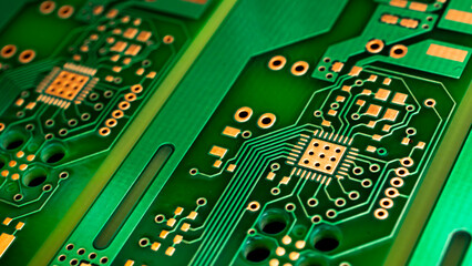
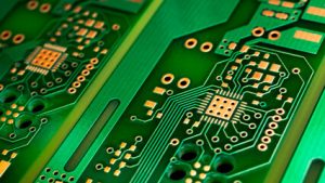
A double-sided PCB is a printed circuit board with copper conductive layers on both the top and bottom sides. Unlike a single-sided PCB, both sides can be used for circuit routing and component placement, allowing designers to create more compact and electrically complex circuits.
The two copper layers are interconnected through plated through-holes and vias, enabling electrical signals and power to pass between the top and bottom layers. This structure provides significantly greater routing flexibility than single-sided boards while remaining more economical and easier to manufacture than many multilayer PCB designs.
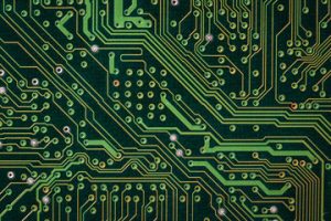
A double-sided board can support a wide range of materials, surface finishes, solder mask colors, copper weights, and board thicknesses. Depending on the application, common materials include FR-4 and high-Tg laminates.
For customers requiring complete manufacturing support, GOPCBA provides integrated PCB manufacturing and assembly solutions, from PCB fabrication and component sourcing to SMT, through-hole assembly, inspection, and testing. PCB Manufacturing and Assembly Services
Key Advantages of Double-Sided PCBs
Double-sided PCBs offer a practical balance between circuit density, manufacturing cost, reliability, and design flexibility.
Higher Circuit Density
Because conductive traces can be routed on both sides of the board, designers have considerably more space for signal routing and power distribution. This makes double-sided boards suitable for applications where a single-sided PCB cannot accommodate the required circuit complexity.
Better Design Flexibility
Components can be mounted on either side of the board, depending on the design requirements. Designers can use the top layer for major components and the bottom layer for additional components, routing, or supporting circuits.
More Efficient Routing
Through-hole vias allow electrical connections between the two copper layers. This makes it easier to route signals around components and reduces the need for long or complicated traces.
Cost-Effective Manufacturing
For many electronic products, a double-sided PCB provides sufficient circuit density without the additional manufacturing cost associated with multilayer construction. It is therefore widely used for prototypes, low-volume production, and mass-produced electronic products.
Suitable for Automated Assembly
Double-sided boards can be manufactured and assembled using modern SMT and through-hole production processes. GOPCBA supports double-sided SMT assembly as well as mixed SMT and THT production for more complex products. PCB Assembly Services
Double-Sided PCB Manufacturing Process
The manufacturing process of a double-sided PCB involves several controlled production stages. Proper material selection, circuit imaging, drilling, copper plating, solder mask application, surface finishing, and electrical inspection all contribute to the final board’s performance and reliability.
1. Material Preparation
The process begins with the selection of an appropriate PCB laminate according to the electrical, thermal, mechanical, and environmental requirements of the application.
FR-4 is one of the most commonly used materials for general-purpose double-sided boards. For demanding applications, high-Tg, high-frequency, or other specialized laminates may be selected.
2. Circuit Imaging and Etching
The circuit pattern is transferred onto the copper surfaces of the PCB. Unwanted copper is then removed through controlled chemical processing, leaving the required conductive traces and pads.
3. CNC Drilling and Through-Hole Formationdouble-sided PCB assembly,
Holes are drilled according to the PCB design. These holes may be used for component leads, vias, mounting points, and electrical connections between the top and bottom copper layers.
4. Copper Plating
The drilled holes are metallized so that electrical connections can be established between the two conductive layers. Additional copper plating may then be applied to achieve the required copper thickness and manufacturing specifications.
5. Solder Mask and Silkscreen
A solder mask is applied to protect exposed copper areas and reduce the possibility of solder bridges during assembly. Silkscreen markings can then be added for component references, polarity indicators, logos, and other assembly information.
6. Surface Finishing
Depending on the application, surface finishes such as HASL, lead-free HASL, ENIG, OSP, or immersion tin may be used. The selected finish affects solderability, surface durability, storage life, and assembly performance.
7. Electrical and Visual Inspection
Finished boards undergo visual inspection and electrical testing to identify manufacturing defects such as open circuits, short circuits, incorrect dimensions, or other process-related problems.
For projects requiring PCB fabrication together with assembly and testing, GOPCBA offers a one-stop manufacturing approach that integrates PCB production, component procurement, assembly, and quality inspection. Components Procurement Services
Double-Sided PCB Assembly Methods
The assembly method selected for a double-sided PCB depends on component type, component density, thermal requirements, board design, and production volume.
Double-Sided SMT Assembly
Surface mount technology is widely used for compact and high-density double-sided boards. Components can be placed on both sides of the PCB, allowing manufacturers to maximize available board space.
A typical process includes solder paste printing, component placement, reflow soldering, inspection, board flipping, and assembly of the second side.
For advanced assemblies, automated optical inspection, X-ray inspection, and electrical testing can be incorporated into the production process.
Through-Hole Assembly
Through-hole technology is commonly used for components that require strong mechanical connections or higher current-handling capability, such as connectors, transformers, power components, and certain electromechanical devices.
Through-hole components may be assembled manually or through automated processes such as wave soldering or selective soldering.
Mixed Technology Assembly
Many modern electronic products combine SMT and through-hole components on the same double-sided PCB. This approach allows manufacturers to use compact SMT components while retaining the mechanical strength of through-hole components where necessary.
GOPCBA provides double-sided PCB assembly together with SMT, THT, and mixed-technology manufacturing capabilities for complex electronic products. Mixed Technology PCB Assembly
Double-Sided PCB Soldering Considerations
Successful assembly of a double-sided board requires careful control of solder paste printing, component placement, thermal profiles, board support, and inspection.
Reflow Soldering
For double-sided SMT assembly, solder paste is normally applied to the first side and components are placed before the board passes through a controlled reflow profile. The board is then processed on the opposite side.
The thermal profile must be carefully developed according to the PCB construction and component specifications. Particular attention should be given to large components, heavy copper areas, thermal masses, and components with strict temperature limitations.
Selective and Wave Soldering
When a board contains through-hole components, selective soldering or wave soldering may be used depending on the product design.
Selective soldering applies molten solder only to designated through-hole solder joints, helping protect nearby SMT components and reducing unnecessary thermal exposure.
Inspection and Testing
Inspection is an important part of the assembly process. Depending on product requirements, manufacturers may use solder paste inspection, AOI, X-ray inspection, ICT, functional testing, and final visual inspection.
GOPCBA provides inspection and testing capabilities throughout the PCBA manufacturing process, helping customers verify solder quality, component placement, electrical performance, and overall product reliability. PCB Assembly Testing & Quality Assurance
Applications of Double-Sided PCBs
Because of their balance between cost and circuit density, double-sided PCBs are used across a broad range of electronic products.
Industrial Electronics
Industrial controllers, automation equipment, sensors, motor controllers, instrumentation, and data acquisition systems often use double-sided boards where reliable circuit routing and stable operation are required.
Automotive Electronics
Double-sided PCBs can be used in automotive control modules, instrument systems, lighting electronics, power management equipment, and other electronic subsystems.
Power Electronics
Power supplies, LED drivers, battery-related electronics, converters, and control circuits can use double-sided PCB construction when the required power and thermal characteristics can be achieved with the selected materials and copper thickness.
Communication Equipment
Routers, communication modules, signal-processing equipment, and other electronic communication products can benefit from the additional routing area provided by two conductive layers.
Consumer Electronics
Home appliances, control panels, audio equipment, smart devices, and other consumer products frequently use double-sided PCBs for their combination of compact design and manufacturing efficiency.
Medical Electronics
Medical and healthcare electronic equipment may use double-sided PCB assemblies where the circuit complexity and reliability requirements are compatible with a two-layer construction.
GOPCBA supports PCB assembly solutions for industrial, medical, automotive, IoT, communication, and other demanding electronic applications. Why Choose GOPCBA
Double-Sided PCB vs. Single-Sided PCB
The primary difference is the number of conductive layers available for circuit routing.
A single-sided PCB has copper circuitry on one side only, making it suitable for relatively simple and cost-sensitive electronic products. A double-sided PCB provides copper circuitry on both sides and uses plated through-holes or vias to establish electrical connections between the layers.
As circuit complexity increases, double-sided construction provides greater routing flexibility and component density without immediately requiring a multilayer PCB.
For many applications, the choice depends on circuit complexity, board size, component count, electrical requirements, production volume, and target cost.
Design Considerations for Double-Sided PCBs
A successful double-sided PCB design should consider both electrical performance and manufacturability from the beginning of the project.
Component Placement
Component placement should allow sufficient clearance for assembly equipment, soldering processes, inspection, rework, and thermal management.
Via and Trace Design
Trace width, spacing, via dimensions, annular rings, and copper thickness should be selected according to the electrical requirements and manufacturing capabilities of the PCB supplier.
Thermal Management
High-power components may require larger copper areas, thermal vias, heat sinks, or alternative PCB materials to control operating temperature.
DFM Review
Design for Manufacturing (DFM) review can identify potential problems before production begins. These may include insufficient spacing, unsuitable drill sizes, component clearance issues, solder mask problems, or assembly constraints.
GOPCBA provides engineering and DFM support to help customers identify manufacturing risks before production and improve overall product manufacturability.
Quality Control for Double-Sided PCBs
Reliable PCB assembly requires quality control throughout the entire manufacturing process rather than relying only on final inspection.
A comprehensive quality system may include:
- Incoming material inspection
- PCB dimensional and visual inspection
- Solder paste inspection
- Automated optical inspection
- X-ray inspection for hidden solder joints
- First article inspection
- In-circuit testing
- Functional testing
- Final inspection
- Production traceability
GOPCBA integrates manufacturing, assembly, inspection, and testing processes to provide customers with a more consistent production workflow. Contact GOPCBA for a PCB Project
Why Choose GOPCBA for Double-Sided PCB Manufacturing and Assembly?
Choosing the right manufacturing partner is important when a double-sided PCB must meet strict requirements for quality, reliability, delivery, and cost.
GOPCBA provides integrated PCB manufacturing and PCBA services, covering PCB fabrication, component procurement, SMT assembly, through-hole assembly, mixed-technology assembly, inspection, testing, and final integration.
The integrated manufacturing model helps reduce communication between multiple suppliers and simplifies project management from prototype development through production.
Customers can also benefit from engineering support, DFM review, component sourcing, automated assembly, quality inspection, and flexible production capabilities.
Conclusion
A double-sided PCB provides an effective solution for electronic products that require more circuit routing space and component density than a single-sided board can offer, without necessarily requiring the complexity and cost of a multilayer PCB.
With two copper layers, plated through-holes, flexible component placement, and compatibility with SMT and through-hole technologies, double-sided boards can support a wide variety of industrial, automotive, communication, power, medical, and consumer electronics applications.
For projects requiring dependable double-sided PCB manufacturer capabilities, integrated fabrication, assembly, component sourcing, inspection, and testing can provide a more efficient path from PCB design to finished electronic product. GOPCBA offers one-stop PCBA manufacturing solutions for prototype, low-volume, and production requirements.