What Is a 3D Printed Circuit Board?
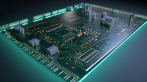
A 3D Printed Circuit Board is an electronic circuit manufactured using additive manufacturing techniques rather than relying entirely on conventional PCB fabrication processes. Unlike traditional flat circuit boards, 3D PCB technology can create conductive paths and electronic structures on or around three-dimensional surfaces.
This approach makes it possible to integrate electronic functions into products with curved, irregular, or space-constrained geometries. It is particularly interesting for applications where conventional flat PCBs, onnectors, or wiring cmay limit product design.
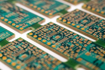
Traditional Printed Circuit Board Manufacturing typically involves processes such as imaging, etching, lamination, drilling, plating, and solder-mask application. By comparison, 3D PCB printing can use additive processes to deposit insulating and conductive materials in controlled patterns.
For production-ready electronic products, conventional PCB fabrication and assembly remain important because they provide established materials, high reliability, controlled electrical performance, and scalable manufacturing. GOPCBA provides professional PCB manufacturing services for prototype and volume-production requirements. (GOPCBA)
What Materials Are Used for 3D Printed PCBs?
The materials used in 3D PCB Printing depend on the manufacturing method and electrical requirements. Common material categories may include:
- Conductive inks or conductive polymers
- Thermoplastic or polymer substrates
- Copper-based conductive materials
- Insulating dielectric materials
- Conventional copper-clad laminate materials
- Specialized materials designed for additive electronics manufacturing
Material selection is critical because electrical conductivity, adhesion, thermal stability, dimensional accuracy, and mechanical strength all affect PCB performance.
For applications that require established PCB materials and controlled manufacturing specifications, conventional PCB production remains the preferred approach. Modern PCB manufacturers can support materials and structures ranging from standard FR-4 to flexible, rigid-flex, HDI, aluminum, and other specialized PCB technologies. (GOPCBA)
Advantages of 3D Printed PCB Technology
Cost-Effective Prototyping
One potential advantage of a 3D Printed PCB is the ability to produce customized electronic structures without relying on extensive tooling. This can be useful during early-stage product development, especially when engineers need to evaluate different shapes or circuit configurations quickly.
For projects requiring rapid electronics development, rapid PCBA prototyping can provide another practical route from design files to assembled prototypes. GOPCBA supports SMT and through-hole assembly, component procurement, testing, and rapid prototype production. (GOPCBA)
Reduced Material Waste
Additive manufacturing deposits material where it is needed rather than removing large quantities of material through conventional subtractive processes. This can potentially reduce material waste and enable more compact electronic structures.
Faster Design Iteration
Because additive manufacturing can support direct digital production, engineers can modify designs and produce new iterations without extensive tooling changes. This is valuable for research, product development, and specialized electronics.
Greater Design Freedom
One of the most attractive characteristics of 3D PCB Printing is its ability to support unconventional geometries. Circuit structures may potentially be integrated into curved surfaces, housings, mechanical components, or other three-dimensional product structures.
On-Demand Production
3D printing can support production without maintaining large inventories of specialized circuit boards. This may be beneficial for prototypes, customized electronics, research projects, and low-volume applications.
For low-volume commercial products, manufacturers can also combine conventional PCB fabrication with flexible production and assembly. Low-volume PCB assembly supports prototype and small-batch requirements across rigid, flexible, rigid-flex, HDI, aluminum, and multilayer PCB technologies. (GOPCBA)
Limitations of 3D Printed PCBs
Electrical Conductivity
One of the main challenges facing 3D-printed electronics is electrical conductivity. Some additive conductive materials may not provide the same conductivity, current-carrying capability, or long-term stability as conventional copper traces.
For demanding electronic applications, copper-based conventional PCB structures remain widely used because of their predictable electrical and thermal performance.
Limited Material Selection
3D-printed electronic materials are developing rapidly, but the available material range may still be narrower than the extensive selection used in conventional PCB manufacturing.
Depending on the application, engineers may need to evaluate dielectric properties, conductivity, thermal expansion, chemical resistance, and environmental stability before selecting a manufacturing technology.
Size and Equipment Constraints
The maximum dimensions of a 3D-printed circuit depend on the available printer, deposition technology, material system, and production process. Complex or large electronic assemblies may therefore require alternative manufacturing methods.
Manufacturing Maturity
Although 3D printing has advanced considerably, it is not a universal replacement for conventional PCB manufacturing. Established PCB processes remain better suited to many commercial applications requiring high production volumes, sophisticated multilayer structures, fine-pitch components, controlled impedance, and stringent reliability requirements.
Modern PCB manufacturing capabilities can support boards from simple designs to advanced HDI structures, including multilayer boards, blind and buried vias, impedance control, and fine geometries. (GOPCBA)
Applications of 3D Printed Circuit Boards
Wearable Electronics
Wearable products often require lightweight and compact electronic structures. 3D Printed Circuit Boards can potentially be integrated into unconventional product geometries, making them suitable for research into smart watches, fitness devices, wearable sensors, and other compact electronics.
Flexible PCB technology is another practical solution for products requiring bending and space-efficient electrical connections. Flex and rigid-flex PCB assembly supports single-sided, double-sided, multilayer, HDI flexible, and rigid-flex PCB assemblies. (GOPCBA)
Medical Electronics
Medical devices frequently require compact and customized electronic structures. 3D-printed electronics may be explored for specialized sensors, wearable medical equipment, assistive devices, and other applications where electronic integration and product geometry are important.
For production medical electronics, however, PCB manufacturing and assembly must meet appropriate quality, reliability, testing, and traceability requirements.
Robotics and Drones
Robots and unmanned systems often have limited internal space and complex mechanical structures. Integrating electronic circuits into three-dimensional components could help reduce wiring, connectors, and unused space.
Conventional PCB assembly remains highly relevant for robotic control systems, motor controllers, sensors, communication modules, and embedded computing hardware.
Internet of Things
IoT devices require compact electronics that can fit inside increasingly small and customized product housings. 3D-printed electronic structures may offer new design possibilities for sensors, smart-home products, wireless devices, and embedded systems.
For commercial IoT products, a professional PCB assembly provider can combine PCB fabrication, component sourcing, SMT, through-hole assembly, testing, and other manufacturing services within one production workflow. (GOPCBA)
Automotive Electronics
Automotive systems increasingly depend on sensors, control modules, communication electronics, and embedded computing. 3D electronic manufacturing may eventually provide additional options for integrating circuits into space-constrained automotive components.
However, automotive electronics generally require high reliability, thermal stability, vibration resistance, and strict manufacturing controls. Conventional PCB technologies therefore remain essential for many automotive applications.
3D Printed PCB vs. Conventional PCB Manufacturing
3D printing and conventional PCB manufacturing serve different purposes.
3D printing is particularly attractive when design freedom, rapid experimentation, unusual geometries, and customized structures are priorities. Conventional PCB manufacturing is generally more suitable when engineers require predictable electrical performance, established materials, multilayer structures, high-volume production, and long-term reliability.
For example, advanced conventional PCB manufacturing can support up to 48-layer boards, fine trace and spacing requirements, laser microvias, controlled impedance, and various PCB material systems. (GOPCBA)
For electronics that require both a fabricated circuit board and assembled electronic components, an integrated manufacturing partner can simplify the production process. GOPCBA supports PCB fabrication, component procurement, SMT/THT assembly, testing, and other electronic manufacturing services. (GOPCBA)
The Future of 3D PCB Printing
The development of 3D Printed PCB technology is closely connected to the broader growth of additive electronics manufacturing. Improvements in conductive materials, printing resolution, multilayer deposition, embedded components, automation, and process control could expand the range of applications.
In the near term, 3D PCB technology is likely to complement rather than completely replace conventional PCB manufacturing. It can provide valuable advantages for customized electronics, rapid experimentation, unconventional geometries, and specialized low-volume applications, while traditional PCB processes continue to dominate many commercial electronic products.
For production projects that require proven manufacturing processes, scalable capacity, and professional assembly, PCBA capabilities include turnkey, partial-turnkey, and kitted/consigned assembly, with support for rigid, flexible, and rigid-flex PCBs and advanced component packages. (GOPCBA)
Conclusion
A 3D Printed Circuit Board represents an emerging approach to electronic manufacturing that combines additive manufacturing with conductive and insulating materials. Its major potential benefits include design flexibility, rapid prototyping, reduced material waste, customized geometries, and on-demand production.
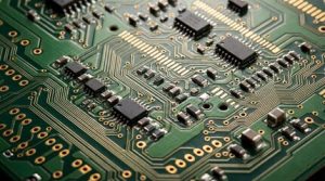
At the same time, limitations involving conductivity, material availability, production size, equipment constraints, and manufacturing maturity mean that 3D PCB technology is not yet a universal replacement for conventional PCBs.
For many commercial electronic products, established Printed Circuit Board Manufacturing combined with professional PCB Assembly remains the most practical route to achieve consistent electrical performance, reliability, and scalable production. As additive electronics technology continues to mature, 3D PCB printing is expected to create new possibilities for next-generation wearable, medical, robotic, IoT, and automotive electronics.