PCB Acceptance Criteria: A Complete Guide to PCB Quality Standards
What Are PCB Acceptance Criteria?
PCB acceptance criteria define the specific characteristics, workmanship requirements, dimensional tolerances, and performance requirements that a printed circuit board must meet before it can be accepted for production or delivery.
A professional PCB inspection process typically evaluates board dimensions and thickness, surface condition, copper thickness, solder mask coverage, silkscreen quality, conductor geometry, drilled holes, pads, board outline, and electrical performance.
For manufacturers and OEMs, clearly defined PCB quality standards are essential for maintaining consistent production quality, reducing manufacturing defects, and ensuring that finished circuit boards perform reliably in their intended applications.
Acceptance requirements should always be determined according to the applicable industry standard, customer drawings, fabrication notes, purchase specifications, and product requirements.
For customers developing a new PCB, a properly controlled PCB manufacturing process is equally important because acceptance quality is influenced by material selection, fabrication processes, dimensional control, surface finishing, and final inspection.
What Is IPC-A-600?
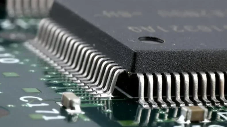
IPC-A-600 is one of the most widely referenced standards for evaluating the acceptability of printed circuit boards. It provides visual and dimensional criteria that help manufacturers, inspectors, engineers, and customers determine whether a PCB meets specified workmanship requirements.
The standard covers numerous PCB characteristics, including:
- Base materials
- Conductors and copper features
- Plated-through holes
- PCB dimensions and tolerances
- Solder mask
- Surface conditions
- Board edges and contours
- Annular rings
- Various visible manufacturing conditions
However, IPC-A-600 should not be treated as a substitute for the customer’s complete fabrication documentation. When a project contains specific dimensional, material, impedance, copper-weight, surface-finish, or reliability requirements, those requirements should be clearly defined in the manufacturing documentation.
A robust PCB inspection program therefore combines applicable IPC requirements with customer-specific specifications.
IPC-A-600 Class 2 vs. Class 3
IPC-A-600 defines different acceptability classes according to the intended application and reliability requirements of the PCB.
Class 2
Class 2 is generally associated with products where continued performance and extended service life are important, but uninterrupted operation is not necessarily critical.
Typical applications may include:
- Consumer electronics
- Commercial electronics
- Communication equipment
- Industrial electronics
- General-purpose electronic products
Class 3
Class 3 is intended for higher-reliability applications where continued performance is critical and equipment downtime may have significant consequences.
Typical applications may include:
- Automotive electronics
- Medical electronics
- Aerospace electronics
- High-reliability industrial systems
- Mission-critical electronic equipment
Class 3 normally requires tighter workmanship control and more stringent acceptance criteria than Class 2. The correct class should therefore be specified according to the product’s application and reliability requirements rather than selected simply because it represents a higher level.
PCB Edge and Board Contour Acceptance Criteria
The PCB edge is an important part of final inspection because excessive damage, cracks, delamination, or rough processing can affect mechanical reliability and potentially expose internal materials or conductive structures.
During PCB manufacturing quality inspection, inspectors should evaluate:
- Board edge damage
- Burrs and rough edges
- Nicks and chips
- Delamination
- Board warpage
- Cutouts and internal contours
- CNC routing quality
- V-cut position and depth
Minor edge roughness may be acceptable when it does not compromise the board structure or electrical performance. However, excessive edge damage, continuous burrs, cracks, or delamination should be rejected.
Board warpage must also remain within the tolerance defined by the applicable specification. For assemblies with demanding mechanical or soldering requirements, excessive warpage can cause problems during component placement and reflow.
PCB Surface Acceptance Criteria
The PCB surface should be clean, uniform, and free from defects that could affect electrical performance, solderability, reliability, or assembly.
Acceptable Surface Conditions
Minor cosmetic marks may be acceptable when they do not affect functionality or violate specified dimensional requirements.
The surface should generally be free from:
- Excessive contamination
- Corrosion
- Delamination
- Blisters
- Cracks
- Significant scratches
- Exposed copper caused by unacceptable damage
- Foreign particles that compromise electrical clearance
Fingerprints, chemical residues, or contamination that can affect solderability or electrical performance should not be accepted.
Surface-finish quality is particularly important for fine-pitch components, BGA packages, high-density designs, and boards requiring long-term reliability.
Solder Mask Acceptance Criteria
The solder mask protects copper conductors and helps prevent solder bridges during assembly. Its coverage, registration, adhesion, and appearance should therefore be carefully controlled.
Solder Mask Registration
Solder mask misregistration must remain within the applicable specification. Excessive movement can reduce pad exposure, cover solderable areas, or expose adjacent copper.
Potential defects include:
- Excessive solder mask offset
- Exposed copper in unintended areas
- Solder mask wrinkles
- Solder mask bubbles
- Peeling
- Cracking
- Poor adhesion
- Excessive solder mask contamination on pads
The acceptable tolerance depends on the PCB design, pad geometry, spacing, and applicable customer or industry requirements.
Solder Mask Surface Defects
Minor cosmetic scratches may be acceptable if they do not expose copper or compromise insulation. Scratches that expose conductive material, create a potential short circuit, or reduce required clearance should be rejected.
Bubbles, peeling, cracking, or significant solder mask defects should also be evaluated against the applicable IPC-A-600 requirements and customer specifications.
Copper Trace Acceptance Criteria
Copper traces are fundamental to PCB electrical performance. During inspection, the conductor width, spacing, shape, surface condition, and continuity should be evaluated against the approved PCB fabrication data.
Typical defects include:
- Excessively narrow traces
- Excessive conductor spacing variation
- Copper scratches
- Conductor nicks
- Burrs
- Short circuits
- Open circuits
- Improper repairs
- Excessive copper loss
A damaged conductor may be unacceptable when the remaining copper width falls below the specified minimum or when the defect affects electrical performance.
For high-density PCBs, small changes in conductor geometry can significantly affect impedance, current capacity, and signal integrity. This makes accurate fabrication and dimensional inspection especially important.
Through-Hole and Via Acceptance Criteria
Through-holes and vias must be inspected for dimensional accuracy, plating quality, cleanliness, and structural integrity.
Common defects include:
- Blocked holes
- Incorrect hole diameter
- Missing holes
- Extra holes
- Mislocated holes
- Poor plating
- Voids
- Cracks
- Excessive burrs
- Damaged annular rings
A blocked or undersized hole can prevent component insertion or interfere with mechanical assembly. Incorrect hole positioning can also create alignment problems between the PCB and other components.
For plated-through holes, barrel integrity and plating quality are especially important because the plated structure provides electrical connections between PCB layers.
Solder Pad Acceptance Criteria
Solder pads must provide a clean and reliable surface for component attachment.
Inspection should focus on:
- Pad dimensions
- Pad location
- Pad surface finish
- Oxidation
- Plating condition
- Scratches and nicks
- Contamination
- Solder mask encroachment
- Pad lifting or damage
Pads should be free from contamination that could interfere with soldering. Excessive scratches, missing plating, oxidation, or damaged pad geometry can reduce solderability and assembly reliability.
For BGA and fine-pitch components, even relatively small pad defects can have a significant impact on solder-joint quality.
Carbon Ink, Peelable Mask, and High-Temperature Mask
Some PCBs require additional materials or processing features such as carbon ink, peelable solder mask, or high-temperature masking.
These features must remain correctly positioned and must not interfere with electrical connections, component mounting areas, or other manufacturing operations.
Typical defects include:
- Carbon ink short circuits
- Incorrect carbon ink location
- Peelable mask covering unintended areas
- Holes or breaks in the masking material
- High-temperature mask extending into prohibited areas
- Mask contamination on solderable areas
Acceptance should always be based on the customer’s drawings and process requirements.
PCB Outline and Shape Acceptance Criteria
The finished PCB outline must match the approved manufacturing data.
Inspection should verify:
- Overall length and width
- Board thickness
- Hole locations
- Cutouts
- Slots
- V-cut position
- V-cut depth
- CNC routing
- Edge profile
- Gold finger bevel
- Mechanical tolerances
An incorrect board outline can prevent the PCB from fitting into its enclosure or mating correctly with connectors and other mechanical components.
V-cut processing should also be carefully controlled. Excessive depth can weaken the board and cause cracking, while insufficient depth may make depanelization difficult.
For gold-finger PCBs, bevel angle, bevel depth, edge condition, and plating integrity should be checked against the approved specification.
Electrical Testing and Final PCB Inspection
Visual inspection alone cannot verify every aspect of PCB quality. Depending on the product and customer requirements, electrical testing may also be necessary.
Typical electrical tests include:
- Continuity testing
- Isolation testing
- Short-circuit testing
- Open-circuit testing
- Impedance testing
- Flying probe testing
- Other customer-specific electrical tests
For assembled boards, additional PCBA testing may include ICT, FCT, X-ray inspection, AOI, and other functional or reliability tests.
PCBA Testing can be incorporated into the manufacturing process when electrical performance and assembly functionality must be verified beyond bare-board visual inspection.
How to Build an Effective PCB Quality Inspection Process
A reliable quality system should not rely only on final inspection. Quality should be controlled throughout the complete manufacturing process.
A typical process can include:
- Engineering document review
- Material verification
- PCB fabrication process control
- Dimensional inspection
- Visual inspection
- Surface-finish inspection
- Solder mask inspection
- Hole and via inspection
- Electrical testing
- Final quality inspection
- Packaging and shipment verification
For more complex PCBs, additional inspection methods may be required according to product requirements.
A comprehensive PCB quality standards system should also establish clear inspection records, defect classification, corrective actions, and traceability.
Why PCB Manufacturing Quality Matters
PCB defects can create problems far beyond the circuit board itself. A dimensional error may prevent assembly, while an electrical defect can cause intermittent failures or complete product malfunction.
Poor manufacturing quality can also result in:
- Increased rework
- Higher production costs
- Delayed product launches
- Assembly problems
- Field failures
- Customer returns
- Reduced product reliability
This is why experienced manufacturers combine engineering review, process control, inspection, and testing throughout the production cycle.
PCB Manufacturing provides a useful overview of PCB fabrication capabilities, materials, surface finishes, and manufacturing options.
PCB Acceptance Criteria Checklist
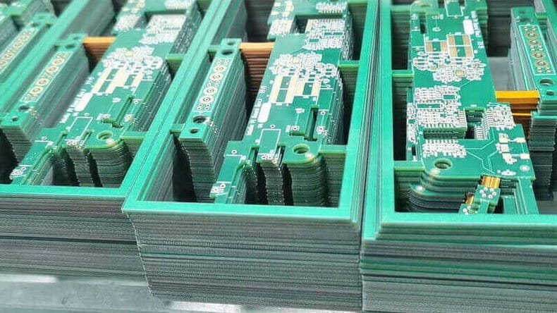
Before accepting a PCB shipment, customers and quality engineers should verify the following:
- Board dimensions comply with approved drawings
- PCB thickness is within specification
- Copper thickness meets requirements
- Board surface is free from unacceptable defects
- Solder mask registration is acceptable
- Silkscreen is clear and correctly positioned
- Trace width and spacing meet design requirements
- Holes are correctly positioned and sized
- Plated holes are structurally sound
- Pads are clean and solderable
- Board outline matches the approved design
- V-cuts and slots meet specifications
- Gold fingers meet dimensional and plating requirements
- Electrical tests meet the specified requirements
- Packaging protects the boards during transportation
For projects requiring tighter quality control, customers can also review the manufacturer’s documented Quality Management procedures and inspection capabilities.
Choosing a PCB Manufacturing Partner
When selecting a PCB supplier, price should not be the only consideration. A reliable supplier should demonstrate appropriate engineering capability, manufacturing capacity, inspection procedures, material control, testing capability, and quality-system management.
Key factors to evaluate include:
- Manufacturing experience
- PCB fabrication capabilities
- Material availability
- Surface-finish options
- Dimensional control
- Inspection equipment
- Electrical testing
- Quality certifications
- Traceability
- Engineering support
- Production lead time
- Communication and after-sales service
A manufacturer capable of integrating fabrication, assembly, component sourcing, testing, and inspection can also simplify supply-chain management.
For projects requiring higher manufacturing integration, customers may consider turnkey PCB assembly, where PCB fabrication, component sourcing, assembly, testing, and related manufacturing services are coordinated through one supplier.
For prototype and early-stage development, rapid PCBA prototyping can help engineering teams validate circuit functionality and identify manufacturing problems before entering volume production.
PCB Acceptance Criteria: Final Considerations
A well-defined PCB acceptance criteria system provides a common quality baseline for PCB manufacturers, engineers, purchasing teams, and customers.
IPC-A-600 is an important reference for PCB acceptability, but successful quality control also requires compliance with approved drawings, Gerber data, fabrication specifications, material requirements, electrical requirements, and customer-specific standards.
The most effective approach is to establish acceptance requirements before production begins and apply consistent inspection throughout fabrication and testing. This reduces ambiguity, minimizes defects, improves manufacturing consistency, and helps ensure that the finished PCB performs reliably in its intended application.
For customers looking for an integrated manufacturing partner, PCB manufacturing, assembly, component sourcing, inspection, and testing can be coordinated as part of a complete electronics manufacturing workflow.
If you are preparing a new PCB project, provide the Gerber files, BOM, drawings, specifications, and testing requirements so the manufacturing team can review the project and determine the appropriate production and inspection requirements.