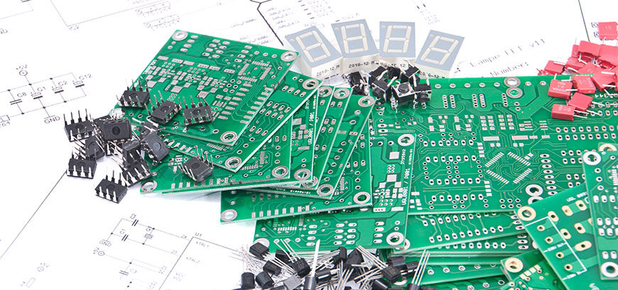
PCB Assembly Acceptance Criteria
What Are PCB Assembly Acceptance Criteria?
PCB Assembly Acceptance Criteria define the visual, mechanical, soldering, and workmanship requirements used to determine whether a finished printed circuit board assembly meets its specified quality level.
A reliable PCB assembly inspection process begins with verifying that all components are compatible with the PCB design and manufacturing requirements. Components must have the correct electrical, mechanical, thermal, and dimensional characteristics for the application.
Component placement is another important part of PCB Assembly Quality. Components must be positioned correctly according to the assembly drawing, PCB layout, polarity markings, and component orientation requirements. Leads, terminals, and solderable ends should properly align with their corresponding pads to establish reliable electrical and mechanical connections.
Solder joints must also meet the applicable acceptance criteria. The solder should provide adequate wetting, coverage, shape, and mechanical integrity without creating shorts, bridges, insufficient solder joints, or other defects.
Finally, the completed assembly should be inspected to confirm that components, solder joints, PCB surfaces, markings, and workmanship conform to the approved design documentation and applicable industry requirements.
For professional PCB manufacturing, IPC-A-610 is one of the most widely recognized references for determining the acceptability of electronic assemblies.
For complete manufacturing requirements, customers can also review our PCB Manufacturing capabilities and processes. PCB Manufacturing
What Is IPC-A-610?
IPC-A-610 is the widely recognized industry standard for the acceptability of electronic assemblies. It provides visual acceptance criteria for electronic assemblies and defines workmanship conditions that can be evaluated during manufacturing inspection.
The standard classifies electronic products into three general product classes:
- Class 1 – General Electronic Products
- Class 2 – Dedicated Service Electronic Products
- Class 3 – High-Reliability Electronic Products
The appropriate class should be selected according to the intended application, operating environment, expected service life, and reliability requirements.
Class 2 is commonly associated with products where continued performance and extended service life are important, while Class 3 applies to products where continued high performance or performance-on-demand is critical and equipment downtime or failure can have serious consequences.
The acceptance criteria can vary according to the applicable IPC-A-610 revision, product class, component package, assembly technology, and customer-specific requirements. Therefore, the applicable standard and revision should always be established before production begins.
Which PCB Assembly Inspection Standards Should Be Followed?
A professional inspection program should establish the applicable PCB Assembly Inspection Standards before manufacturing begins.
Typical requirements include:
- Approved PCB fabrication drawings
- Assembly drawings
- Bill of Materials (BOM)
- Pick-and-place data
- Component datasheets
- Customer-specific workmanship requirements
- Applicable IPC standards
- Electrical and functional test requirements
- Packaging and handling requirements
Inspection can include incoming material inspection, solder paste inspection, automated optical inspection, X-ray inspection, visual inspection, electrical testing, and functional testing.
A complete PCB Assembly Quality system should control quality throughout the entire manufacturing process rather than relying only on final inspection.
For example, production may follow a sequence such as:
IQC → SPI → SMT/THT Assembly → AOI → X-Ray → ICT/FCT → OQC
This process allows potential defects to be identified as early as possible.
You can also review our Quality Management process for more information about pre-production checks, DFM review, process control, and inspection. Quality Management
IPC-A-610 Class 2 vs. Class 3
The difference between Class 2 and Class 3 is primarily related to the required level of reliability and the consequences of product failure.
| Aspect | IPC-A-610 Class 2 | IPC-A-610 Class 3 |
|---|---|---|
| Reliability requirement | Standard | High |
| Typical applications | Consumer electronics, communications, computers, industrial controls | Medical, aerospace, military, automotive, high-reliability systems |
| Workmanship requirements | Controlled acceptance criteria | More stringent acceptance criteria |
| Inspection requirements | Appropriate for general dedicated-service products | More rigorous for high-reliability products |
| Cost | Generally lower | Generally higher |
The correct product class should be determined during the engineering and quotation stage rather than after production begins.
A consumer product may not require the same acceptance level as a mission-critical medical, aerospace, or defense electronic assembly. Applying unnecessarily strict criteria can increase manufacturing costs, while applying insufficient criteria can create reliability risks.
Detailed PCB Assembly Acceptance Criteria
The following sections summarize common inspection areas used when evaluating PCB Assembly Acceptance Criteria.
Component Alignment and Offset
Component placement accuracy is particularly important for SMT components with small packages and fine-pitch terminals.
For acceptable placement, the solderable end of a component should adequately overlap the PCB pad. Excessive side-to-side displacement can reduce the effective solder joint area and negatively affect electrical and mechanical reliability.
Typical inspection considerations include:
- Side offset
- End offset
- Pad overlap
- Solderable termination overlap
- Component orientation
- Polarity
- Clearance from adjacent components
For certain chip components, the side offset should not exceed the applicable percentage of the smaller component termination or pad width.
End offset requirements are also evaluated according to the component package and applicable acceptance class.
An assembly may be considered unacceptable when the solderable termination moves outside the intended pad area or when the remaining solderable area is insufficient to provide a reliable connection.
Solder Volume and Solder Joint Formation
Solder volume is a critical part of PCB Assembly Quality.
Insufficient solder can reduce mechanical strength and electrical reliability. Excessive solder can increase the risk of solder bridging, shorts, and interference with adjacent components.
Inspection should consider:
- Solder joint width
- Solder joint height
- Solder coverage
- Wetting
- Solder fillet formation
- Component termination coverage
- Pad coverage
For chip components, the acceptable solder joint generally requires sufficient overlap between the component termination and PCB pad.
The solder joint should also provide adequate vertical and horizontal coverage without extending onto areas where it could cause electrical or mechanical problems.
Side Overhang, Component Tilt, and End-Termination Conditions
Surface-mount components must be positioned so that their solderable terminals maintain sufficient contact with the corresponding PCB pads.
Potential defects include:
- Excessive side overhang
- Component rotation
- Terminal deformation
- Insufficient solderable contact
- Poor wetting
- Component body interference
- Improper orientation
Component tilting can also occur when solder volume, pad design, component geometry, or reflow conditions are not properly balanced.
One common example is tombstoning, where one end of a small passive component lifts from the PCB during reflow soldering.
Tombstoning can result from unequal solder forces, pad geometry, thermal imbalance, or differences in solder paste deposition.
Castellated Components
Castellated components require special attention because their solderable areas are formed along the edges of the package.
Inspection normally evaluates:
- Side offset
- End offset
- Solder joint width
- Solder joint height
- Wetting
- Pad overlap
The component should maintain adequate overlap with the PCB pad, and the solder joint should provide sufficient contact area.
Excessive lateral displacement can reduce the effective soldering area and may result in an unacceptable connection.
Flat, L-Shaped, and Gull-Wing Leads
Lead alignment is a major inspection item for packages such as QFP, SOIC, and similar devices.
The inspection should evaluate:
- Lead side offset
- Toe extension
- Heel solder joint
- Side solder joint
- Lead coplanarity
- Lead deformation
- Solder coverage
- Electrical clearance
The maximum acceptable side offset depends on the applicable lead geometry and acceptance class. In many cases, the allowable offset is evaluated against the lead width and a defined maximum dimensional limit.
Toe overhang must also maintain the required minimum electrical clearance from adjacent conductors.
For side solder joints, the required soldered length depends on the relationship between lead length and lead width.
If the lead length is less than three times its width, the applicable minimum solder joint length is based on the lead length.
If the lead length exceeds three times the lead width, the applicable requirement is determined using the relevant lead dimensions and acceptance criteria.
Heel Solder Joint and Lead Coplanarity
The heel portion of a gull-wing lead should have sufficient solder coverage to establish a reliable connection without creating excessive solder accumulation.
The solder joint should extend appropriately along the lead while avoiding undesirable solder on the component body.
Lead coplanarity is also important because all leads must make adequate contact with the PCB during soldering.
A misaligned or lifted lead can cause:
- Open circuits
- Weak solder joints
- Intermittent electrical connections
- Insufficient solder coverage
- Mechanical reliability problems
Proper component placement and controlled reflow profiles are therefore essential to achieving consistent SMT Assembly quality.
For more information about surface-mount manufacturing, see our SMT PCB Assembly service. SMT PCB Assembly
BGA and Array Component Inspection
BGA components require additional inspection because many solder joints are hidden underneath the package and cannot be fully evaluated through conventional visual inspection.
The primary objectives include:
- Correct BGA placement
- Proper solder ball alignment
- Adequate solder connection
- No solder bridging
- No open solder joints
- No incomplete reflow
- No excessive voiding where applicable
- Consistent solder joint formation
X-ray inspection is commonly used to evaluate hidden BGA solder joints.
A properly formed BGA assembly should have solder connections that are sufficiently formed and free from unacceptable bridging or incomplete reflow.
Common BGA defects include:
- Solder bridging
- Incomplete solder reflow
- Open solder joints
- Poor solder ball collapse
- Excessive voiding
- Misalignment
- Insufficient solder connection
For complex assemblies, X-ray inspection can provide information that cannot be obtained through conventional visual inspection alone.
Soldering Defects: Pinholes, Voids, Cold Solder, and Non-Wetting
Solder wetting is a fundamental requirement for reliable solder joints.
A properly formed solder joint should demonstrate adequate wetting between the solder and the surfaces being joined.
Common soldering problems include:
Pinholes and Voids
Small holes or voids may occur within solder joints due to trapped gases, flux activity, PCB surface conditions, solder paste characteristics, or reflow parameters.
The significance of voids depends on their size, location, quantity, component type, and application.
Cold Solder Joints
A cold solder joint may exhibit poor solder flow, poor bonding, an irregular surface, or insufficient metallurgical connection.
Possible causes include:
- Insufficient heating
- Incorrect reflow profile
- Contaminated surfaces
- Inadequate solder paste
- Poor process control
Non-Wetting
Non-wetting occurs when solder fails to properly bond to the intended surface.
Potential causes include:
- Oxidation
- Contamination
- Incorrect soldering temperature
- Poor surface finish
- Insufficient flux activity
- Inadequate process parameters
These conditions must be evaluated according to the applicable PCB Assembly Inspection Standards.
Solder Balls, Solder Bridges, and Solder Webbing
Solder balls and solder bridges are common soldering defects that can create electrical reliability problems.
Solder Balls
Solder balls should not violate required minimum electrical clearances or create an unacceptable reliability risk.
Depending on the applicable acceptance criteria, isolated solder particles may be treated differently depending on their location, attachment, and relationship to electrical conductors.
Solder Bridges
A solder bridge occurs when solder unintentionally connects two electrically separate conductors.
Solder bridges can cause:
- Short circuits
- Functional failures
- Excessive current
- Component damage
- Safety risks
Any solder bridge that violates the applicable electrical clearance or creates an unintended connection should be considered unacceptable.
Solder Webbing
Solder webbing refers to thin or irregular solder connections extending between areas that should remain electrically separated.
Proper stencil design, solder paste volume, PCB layout, component spacing, and reflow control help minimize these defects.
Solder Cracks, Disturbed Solder, and Solder Protrusions
Solder joints must remain mechanically stable after soldering.
Potential defects include:
- Solder cracks
- Disturbed solder joints
- Sharp solder protrusions
- Excessive solder
- Solder extending into prohibited areas
- Solder connections that violate electrical clearance
Solder cracking can result from mechanical stress, thermal cycling, poor solder joint formation, component movement, or PCB flexing.
Any solder condition that compromises electrical spacing, mechanical integrity, or long-term reliability should be investigated and evaluated against the applicable acceptance requirements.
Component Damage
Component condition should be inspected before, during, and after assembly.
Acceptable cosmetic damage depends on the component type and the applicable acceptance criteria. However, damage must not compromise the component’s form, fit, function, electrical performance, mechanical integrity, or environmental protection.
Inspection should include:
- Component body
- Terminations
- Leads
- Package surface
- Markings
- Seals
- Connectors
- Insulating materials
Examples of potentially unacceptable damage include:
- Cracks
- Broken components
- Exposed functional materials
- Severe dents
- Excessive scratches
- Deformed leads
- Damaged terminals
- Missing plating
- Burn marks affecting function
- Damage affecting sealing or mechanical integrity
Component markings should remain sufficiently clear for identification and traceability.
Why PCB Assembly Inspection Matters
A comprehensive inspection system is essential for maintaining consistent PCB Assembly Quality.
Inspection is not simply a final visual check. It should be integrated into the entire production process.
A professional PCB assembly workflow may include:
- Engineering review
- BOM verification
- PCB inspection
- Component incoming inspection
- Solder paste inspection
- SMT placement
- Reflow soldering
- AOI inspection
- X-ray inspection where required
- Through-hole assembly
- Electrical testing
- Functional testing
- Final inspection
- Packaging and shipment
This approach helps manufacturers identify defects early and maintain process consistency.
For projects requiring combined surface-mount and through-hole technology, our Mixed Technology PCB Assembly service supports both SMT and THT processes. Mixed Technology PCB Assembly
Visual Inspection vs. Automated Inspection
Visual inspection remains an important part of PCB Assembly Acceptance Criteria, especially for checking component orientation, visible solder joints, mechanical conditions, markings, and workmanship.
However, automated inspection technologies provide additional capabilities.
AOI Inspection
Automated Optical Inspection (AOI) can detect many visible assembly defects, including:
- Missing components
- Incorrect components
- Component displacement
- Polarity errors
- Solder bridges
- Insufficient solder
- Excessive solder
- Lead alignment problems
X-Ray Inspection

X-ray inspection is especially useful for hidden solder joints such as BGA, QFN, and other bottom-terminated components.
It can help identify:
- Hidden solder bridges
- Voids
- Open joints
- Incomplete solder connections
- BGA alignment problems
- Solder ball abnormalities
Electrical and Functional Testing
Visual inspection alone cannot confirm that an assembly functions electrically.
Depending on the product, additional testing may include:
- In-Circuit Test (ICT)
- Flying probe testing
- Functional testing (FCT)
- Programming
- Power-on testing
- Communication testing
- Customer-specific testing
PCB Assembly Acceptance Criteria and Customer Requirements
Although IPC-A-610 provides an important industry reference, customer-specific requirements may also apply.
Before production, customers and manufacturers should clearly define:
- Product class
- Applicable IPC revision
- PCB specifications
- Component requirements
- Solder type
- Lead-free requirements
- Surface finish
- Inspection methods
- Electrical test requirements
- Functional test requirements
- Cosmetic requirements
- Packaging requirements
- Traceability requirements
Special requirements should be documented before manufacturing begins to avoid uncertainty during final inspection.
For projects requiring a complete manufacturing solution, our PCB Assembly service covers SMT, THT, mixed technology assembly, component sourcing, inspection, testing, and production support. PCB Assembly
How to Improve PCB Assembly Quality
Improving PCB Assembly Quality requires control of the complete manufacturing chain rather than focusing on a single production step.
Key practices include:
1. Verify Manufacturing Data
The BOM, Gerber files, pick-and-place files, assembly drawings, and component specifications should be checked before production.
2. Perform DFM and DFA Reviews
Design for Manufacturing (DFM) and Design for Assembly (DFA) reviews can identify potential problems before components are ordered or boards enter production.
3. Control Solder Paste Printing
Solder paste volume and alignment directly affect solder joint quality. SPI can help monitor paste deposition before component placement.
4. Optimize Component Placement
Accurate placement is essential for fine-pitch components, BGA devices, QFN packages, and miniature passive components.
5. Control Reflow Profiles
The reflow temperature profile should be appropriate for the PCB, solder paste, component package, and manufacturing process.
6. Use Appropriate Inspection Technologies
AOI, X-ray, ICT, and functional testing should be selected according to product complexity and risk.
7. Maintain Process Traceability
Production records, inspection results, component information, and test data should be maintained to support quality analysis and future production.
Conclusion
Reliable PCB Assembly Acceptance Criteria provide a consistent framework for evaluating electronic assemblies and controlling manufacturing quality.
From component alignment and solder joint formation to BGA inspection, solder defects, component damage, and electrical testing, every stage contributes to final product reliability.
IPC-A-610 remains an important reference for determining electronic assembly acceptability, but the correct product class, standard revision, component technology, and customer-specific requirements should always be established before production.
A strong PCB Assembly Quality system combines engineering review, controlled manufacturing processes, automated inspection, X-ray analysis where required, electrical testing, functional testing, and final quality verification.
Whether the project involves prototypes, low-volume production, or high-volume manufacturing, selecting the appropriate SMT Assembly process and applying clearly defined PCB Assembly Inspection Standards can significantly reduce manufacturing defects and improve long-term product reliability.
For high-volume production requirements, see our High Volume PCB Assembly capabilities. High Volume PCB Assembly
If you have a new PCB or PCBA project, the manufacturing team can review your Gerber files, BOM, pick-and-place data, drawings, and other production requirements to determine the appropriate assembly process and inspection requirements.