The electronics industry is moving toward smaller products, higher component density, shorter production cycles, and increasingly demanding reliability requirements. As these pressures continue to grow, traditional manual manufacturing methods are no longer sufficient for many modern electronic products.
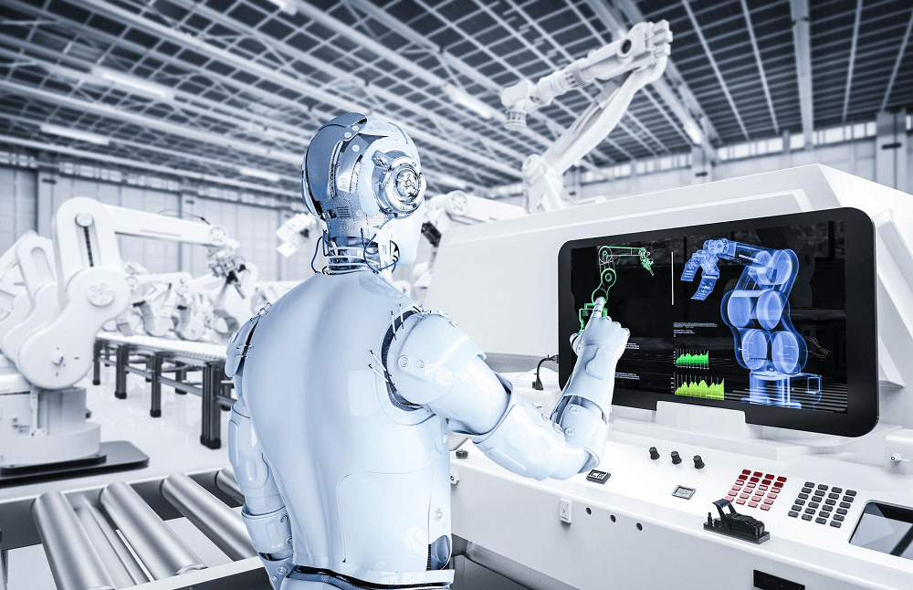
This transformation has accelerated the adoption of PCB assembly automation, robotics in electronics manufacturing, AI in PCB assembly, and smart PCB assembly technologies. Modern production lines are evolving from isolated pick-and-place machines into interconnected manufacturing systems capable of monitoring processes, analyzing production data, detecting defects, and optimizing equipment performance in real time.
For engineers, this transformation offers more than higher production speed. Automated PCB assembly can improve placement accuracy, process consistency, traceability, inspection coverage, and production repeatability. At the same time, artificial intelligence and Industry 4.0 technologies are creating new opportunities for predictive maintenance, intelligent inspection, adaptive process control, and data-driven manufacturing.

This guide explores the evolution of automated PCB assembly, the role of robotics and AI, the practical challenges engineers should consider, and the technologies shaping the future of smart electronics manufacturing.
What Is Automated PCB Assembly?
Automated PCB assembly is the use of automated equipment, software, robotics, and process-control systems to manufacture printed circuit board assemblies with minimal manual intervention.
A modern automated PCB assembly line may integrate:
- Solder paste printing
- 3D solder paste inspection (SPI)
- Automated pick-and-place
- Reflow soldering
- Automated optical inspection (AOI)
- X-ray inspection
- Through-hole insertion
- Selective soldering
- Electrical testing
- Functional testing
- Product traceability
- Manufacturing data collection
The objective is not simply to replace workers with machines. The more important goal is to create a manufacturing process that is repeatable, measurable, traceable, and scalable.
For high-volume production, automation helps maintain consistent process conditions across thousands or millions of boards. For high-mix and low-volume production, flexible automation can reduce changeover time while maintaining production quality.
The Evolution of Automation in PCB Assembly
The early generation of automated PCB assembly primarily focused on increasing the speed of component placement. Modern systems have evolved into interconnected process-control platforms that cover almost the complete SMT manufacturing workflow.
A typical automated SMT process now follows a sequence such as:
Solder Paste Printing → SPI → Pick-and-Place → Reflow → AOI → X-Ray → ICT/FCT
Each stage generates production data that can be analyzed by engineers and manufacturing systems.
From Stand-Alone Machines to Connected Production Lines
Older production environments often treated each machine as an independent workstation. Operators manually moved information between processes, and production problems were frequently discovered only after a downstream inspection step.
Modern smart PCB assembly systems connect machines and production software so that process information can move throughout the line.
For example:
- SPI data can reveal changes in solder-paste deposition.
- Pick-and-place systems can record component placement information.
- Reflow ovens can store thermal profiles.
- AOI systems can classify assembly defects.
- X-ray systems can analyze hidden solder joints.
- MES platforms can associate results with individual PCB serial numbers.
This creates a closed information loop in which production data can be used not only for inspection, but also for process improvement.
Automation and Traceability
Traceability becomes increasingly important as product complexity and regulatory requirements increase.
Modern electronics manufacturers may track:
- Component lot numbers
- PCB batch numbers
- Operator information
- Machine IDs
- Process parameters
- Inspection results
- Test results
- Firmware versions
- Rework records
- Final shipment information
Kingda’s published PCB assembly quality system includes a documented flow from IQC → SPI → SMT/THT Assembly → AOI → X-Ray → ICT/FCT → OQC, together with manufacturing traceability from incoming materials through final shipment.
This connected data structure helps manufacturers perform faster root-cause analysis and determine which products may be affected when a quality problem occurs.
Robotics in Electronics Manufacturing
Robotics are becoming increasingly important in modern electronics manufacturing, particularly where speed, repeatability, precision, or hazardous process conditions are involved.
Robotic Pick-and-Place Systems
High-speed pick-and-place machines are among the most mature examples of robotics in electronics manufacturing.
The machines automatically:
- Retrieve components from feeders.
- Identify component type and orientation.
- Use vision systems to determine PCB position.
- Calculate placement coordinates.
- Place components onto the solder-paste deposits.
- Record placement information for process traceability.
Modern systems can handle extremely small passive components and fine-pitch semiconductor packages.
Kingda’s published SMT capabilities include 01005 passive components, BGA, QFN, CSP, LGA, fine-pitch components, and high-speed automatic component placement, supporting prototype through high-volume production.
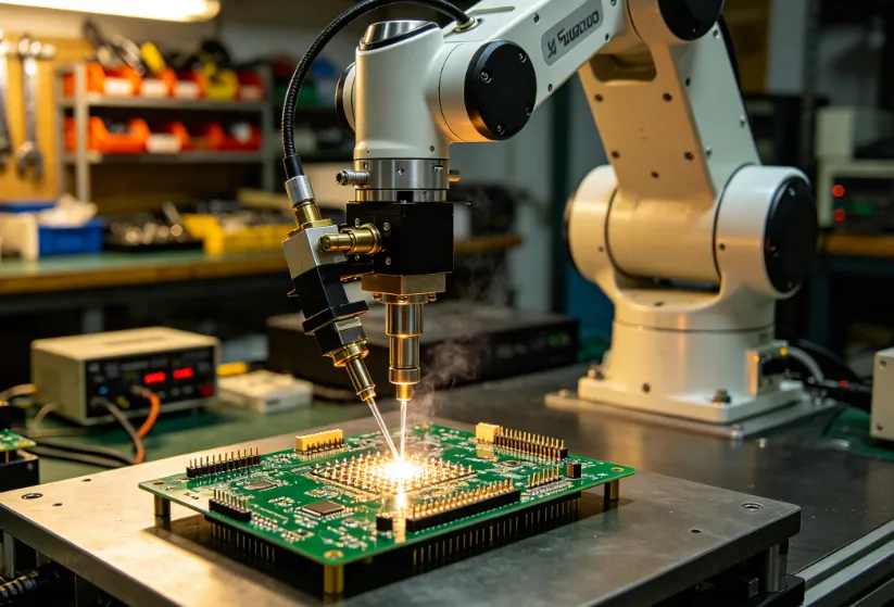
Robotic Soldering
Robotics are also being used for specialized soldering processes.
For through-hole assemblies, selective soldering enables manufacturers to solder specific joints without exposing the entire PCB to a conventional solder wave.
This can be especially useful for mixed-technology assemblies containing:
- SMT components
- Through-hole connectors
- Power devices
- Transformers
- Relays
- Large terminals
Kingda supports wave soldering, selective soldering, manual through-hole assembly, press-fit assembly, and mixed SMT/THT production.
Robotic soldering improves repeatability by controlling parameters such as:
- Soldering temperature
- Contact time
- Solder flow
- Tool position
- Joint location
This reduces variation between operators and can improve process consistency.
AI in PCB Assembly
Artificial intelligence is introducing another layer of intelligence into automated manufacturing.
Traditional inspection systems commonly operate according to predefined rules. AI-based systems can instead learn patterns from large datasets containing examples of acceptable and defective assemblies.
AI-Powered Automated Optical Inspection
AI-powered AOI can improve defect classification by recognizing patterns associated with:
- Solder bridges
- Missing components
- Component displacement
- Incorrect polarity
- Insufficient solder
- Tombstoning
- Abnormal solder fillets
A major advantage is the potential reduction of false positives.
A conventional rule-based inspection system may flag a harmless visual variation as a defect. An AI-based system can learn from historical production data and distinguish normal process variation from genuine quality risks.
However, AI should not replace engineering judgment completely. Critical AI inspection systems still require controlled datasets, validation, periodic monitoring, and human review for uncertain cases.
AI for Predictive Maintenance
Another important application is predictive maintenance.
Instead of waiting for equipment to fail, AI systems can analyze:
- Motor vibration
- Feeder behavior
- Placement accuracy
- Temperature
- Machine cycle time
- Error frequency
- Nozzle performance
- Reflow-system data
The system can identify patterns that indicate a potential equipment problem.
For example, a gradual increase in placement errors may indicate:
- Nozzle wear
- Feeder instability
- Vision-system drift
- Mechanical misalignment
Engineers can then schedule maintenance before the equipment causes a large production interruption.
Smart PCB Assembly and Industry 4.0
Industry 4.0 PCB assembly combines manufacturing equipment, industrial networking, MES, ERP, IoT sensors, data analytics, and automation into one connected manufacturing environment.
The objective is to create a factory where machines do not simply perform operations, but also communicate information about those operations.
MES Integration
A Manufacturing Execution System (MES) can connect:
Material → Production Order → Machine → Process → Inspection → Test → Shipment
This allows individual products to maintain a digital production history.
For example, when a field failure occurs, engineers can potentially determine:
- Which component lot was used.
- Which SMT line built the board.
- Which reflow profile was used.
- Which inspection results were recorded.
- Which operator or shift handled the unit.
- Which firmware revision was installed.
This level of visibility significantly improves quality management and root-cause analysis.
ERP and Supply Chain Integration
ERP integration allows manufacturing systems to connect production requirements with inventory and purchasing.
Automated systems can use production data to improve:
- Component replenishment
- Inventory planning
- Feeder preparation
- Production scheduling
- Material availability
- Supply-chain visibility
For high-volume production, this can help prevent line stoppages caused by material shortages.
The Role of SPI in Automated PCB Assembly
Solder Paste Inspection (SPI) is one of the most important upstream quality-control technologies in SMT assembly.
Before components are installed, 3D SPI systems can measure:
- Paste volume
- Paste height
- Paste area
- Paste position
- Deposit shape
This information helps identify problems such as:
- Insufficient solder paste
- Excessive solder paste
- Misalignment
- Stencil blockage
- Stencil wear
- Printing variation
Because solder-paste quality directly affects subsequent soldering performance, SPI provides an opportunity to detect defects before expensive components are placed.
Kingda lists 3D SPI as part of its PCB assembly inspection capabilities.
Automated Reflow Process Control
Reflow soldering remains one of the most important thermal processes in SMT assembly.
The objective is to heat the PCB and components according to a controlled thermal profile so that the solder paste:
- Preheats gradually.
- Activates flux.
- Reaches the required reflow temperature.
- Forms reliable solder joints.
- Cools at a controlled rate.
Automated reflow systems can record temperature profiles and help engineers maintain process repeatability.
Why Advanced Thermal Profiling Matters
Modern PCBs increasingly combine components with very different thermal masses.
A board may contain:
- Tiny 01005 passives
- Large inductors
- Power semiconductors
- BGA packages
- Large connectors
- Aluminum or copper heat-spreading structures
A single thermal profile therefore cannot always be optimized simply by looking at the oven temperature.
Engineers need to analyze the actual PCB thermal response and validate the process using thermocouples, profiling equipment, and production data.
AOI and X-Ray Automation
Automated inspection is another major pillar of smart PCB assembly.
AOI
Automated Optical Inspection (AOI) is effective for detecting visible assembly defects such as:
- Missing components
- Incorrect components
- Misalignment
- Polarity errors
- Solder bridges
- Tombstoning
- Visible solder defects
X-Ray Inspection
AOI cannot see through packages such as BGA and some QFN structures.
X-ray inspection provides visibility into hidden solder connections and can detect:
- Voids
- Bridging
- Open joints
- Insufficient solder
- Misalignment
- Defective hidden connections
Kingda lists X-ray inspection for BGA and hidden solder joints as part of its inspection capabilities.
Automation for Mixed-Technology PCB Assembly
One of the biggest challenges in modern manufacturing is that not every PCB is purely SMT.
Many products combine:
- SMT
- Through-hole components
- Press-fit connectors
- Large power devices
- Wire harnesses
- Mechanical components
This creates a mixed-technology PCB assembly environment.
The manufacturing line may therefore require:
SMT Printing → SMT Placement → Reflow → THT Insertion → Selective/Wave Soldering → AOI → X-Ray → Testing
Kingda supports mixed SMT/THT assembly, wave and selective soldering, wire harness integration, functional testing, IC programming, and box-build services.
Practical Challenges in PCB Assembly Automation
Automation delivers major benefits, but implementation must be carefully engineered.
1. High Initial Investment
Automated equipment can require substantial capital investment.
A complete SMT line may include:
- Stencil printer
- SPI
- Pick-and-place machines
- Reflow oven
- AOI
- X-ray
- Conveyors
- Material-handling systems
- Testing equipment
The investment must therefore be justified by production volume, product complexity, and expected return.
2. Programming Complexity
Automation does not eliminate engineering work.
Each new PCB may require:
- Machine programming
- Feeder setup
- Pick-and-place optimization
- AOI programming
- SPI programming
- Reflow-profile development
- Test-program development
For high-mix production, reducing changeover time becomes an important manufacturing objective.
3. Miniaturized Components
Components such as 01005 packages require extremely accurate:
- Stencil design
- Solder-paste printing
- Pick-and-place
- Vision inspection
- Reflow control
A small process deviation can create a significant percentage increase in defects.
4. Equipment Maintenance
Automation systems still require preventive maintenance.
Engineers should monitor:
- Nozzle wear
- Feeder performance
- Vision calibration
- Conveyor alignment
- Printer squeegee condition
- Reflow-zone performance
- AOI camera calibration
Maintenance should be scheduled using machine operating data rather than relying only on fixed intervals.
Best Practices for Engineers Implementing Smart PCB Assembly
Successful automation begins during product design.
Design for Manufacturing
DFM should verify that the PCB fits the capabilities of the selected manufacturing process.
Important considerations include:
- Component spacing
- Pad geometry
- Solder-mask clearance
- Panelization
- Component orientation
- Thermal design
- Test access
Design for Assembly
DFA focuses specifically on simplifying and stabilizing the assembly process.
Engineers should consider:
- Component accessibility
- Standardized component packages
- Orientation consistency
- Reduced component variation
- Efficient feeder utilization
- Assembly sequence
Design for Testing
DFT should be considered before manufacturing.
Provide appropriate:
- Test points
- Programming interfaces
- Fixture access
- Boundary-scan access
- Functional test connections
This makes automated testing more practical after assembly.
Use Manufacturing Data as an Engineering Resource
Production data should not be collected simply for reporting.
Engineers should use it to understand:
- First-pass yield
- Defect Pareto
- Rework rate
- Component-related failures
- Process drift
- Machine downtime
- Test failures
Over time, this creates a continuous-improvement loop:
Production Data → Analysis → Corrective Action → Process Optimization → Higher Yield
Kingda’s Automated PCB Assembly Capabilities
For electronics companies looking to implement reliable automated manufacturing, Kingda provides an integrated PCB and PCBA manufacturing platform covering PCB fabrication, component procurement, SMT assembly, THT/DIP assembly, inspection, testing, and final product integration. Kingda was established in 2013 and has developed from PCB fabrication into a one-stop PCBA manufacturing provider.
Automated SMT Production
Kingda’s published capabilities include 8 fully automatic SMT production lines, high-speed component placement, 3D SPI, AOI, X-ray inspection, and controlled reflow processes.
The company supports component packages including:
- 01005
- 0201
- BGA
- QFN
- CSP
- LGA
- Fine-pitch ICs
Its published assembly capability includes BGA packages down to 0.35 mm pitch and fine-pitch components down to approximately 0.38 mm pitch.
Comprehensive Inspection and Testing
Kingda’s published quality-control flow is:
IQC → SPI → SMT/THT → AOI → X-Ray → ICT/FCT → OQC
Inspection and testing options include:
- 3D SPI
- AOI
- X-ray
- FAI
- ICT
- FCT
- Customized testing
This integrated inspection strategy allows process problems to be detected at multiple stages rather than only during final inspection.
Mixed Technology and Box-Build Capability
Kingda also supports mixed-technology PCB assembly, wave and selective soldering, wire harnesses, cable assemblies, IC programming, functional testing, and box-build integration.
This allows customers to manage more of the electronics manufacturing workflow through a single supplier instead of coordinating multiple specialized vendors.
DFM and Engineering Support
Automation works best when manufacturing considerations are incorporated before production begins.
Kingda provides engineering support including:
- DFM
- DFA
- DFX optimization
- BOM validation
- Component sourcing
- Manufacturing process optimization
These engineering activities help identify potential production problems before they become expensive assembly defects.
Prototype-to-Production Scalability
Kingda’s published manufacturing services support prototype, low-volume, medium-volume, and high-volume PCB assembly, allowing customers to move from early engineering validation toward production without changing the fundamental manufacturing partner.
This continuity can be especially valuable for products requiring repeated engineering revisions, traceability, and controlled process transfer.
The Future of PCB Assembly Automation
The next phase of PCB assembly automation will likely focus less on individual machines and more on intelligent cooperation between machines, software, people, and production data.
Several developments are particularly important.
AI-Driven Closed-Loop Manufacturing
Future production systems will increasingly connect inspection information directly to upstream manufacturing processes.
For example:
SPI detects printing drift → AI identifies the trend → Printer parameters are adjusted → AOI confirms improvement
This creates a true closed-loop process rather than a simple inspection system.
Digital Twins
Digital-twin technology can allow engineers to model manufacturing processes virtually before production begins.
This can help optimize:
- Line balancing
- Equipment utilization
- Process sequences
- Material movement
- Changeovers
- Production capacity
Collaborative Robots
Collaborative robots, or cobots, are likely to become more widely used for activities requiring flexibility rather than extreme speed.
Possible applications include:
- Material handling
- Inspection assistance
- Screw fastening
- Packaging
- Rework support
- Prototype production
Lights-Out Manufacturing
The long-term objective of highly automated manufacturing is increasingly lights-out production, where machines handle a large proportion of production with limited human intervention.
However, fully unmanned manufacturing remains highly dependent on product complexity, production volume, equipment integration, maintenance systems, and quality requirements.
Conclusion
PCB assembly automation, robotics, artificial intelligence, and Industry 4.0 technologies are transforming electronics manufacturing from a collection of isolated production processes into an interconnected manufacturing ecosystem.
Automation provides:
Higher Throughput + Better Repeatability + Improved Traceability + Reduced Process Variation
Robotics adds precision and flexibility to component placement, soldering, inspection, and material handling. AI introduces predictive maintenance, intelligent defect classification, and opportunities for closed-loop process control. Industry 4.0 connects machines, MES, ERP, quality systems, and supply-chain data into a unified manufacturing environment.
For engineers, the biggest opportunity is not simply to automate existing processes. It is to redesign the manufacturing workflow around measurable data, intelligent feedback, and manufacturability from the earliest design stage.
Kingda combines automated SMT and THT assembly, advanced inspection, testing, traceability, engineering support, and integrated manufacturing services to support electronics projects from prototype through production.
As electronic products continue to become smaller, faster, and more complex, intelligent smart PCB assembly will become increasingly important. Manufacturers that combine automation with engineering expertise, process discipline, and reliable data management will be better positioned to deliver consistent quality in the next generation of electronics manufacturing.