15 Best PCB Design Companies in 2026: Services, Capabilities, and How to Choose the Right PCB Design Partner
The PCB design company you choose can directly influence whether your electronic product reaches the market on schedule, whether the circuit board performs reliably, and whether it can be manufactured efficiently at scale. A poorly optimized PCB layout can lead to costly redesigns caused by signal integrity, Design for Manufacturability (DFM), thermal management, impedance control, electromagnetic compatibility (EMC), and other engineering issues. These problems can significantly increase development costs and delay time to market.
Professional PCB design services help reduce engineering risks, improve manufacturing yield, accelerate prototyping, and shorten product development cycles.
Although a completed PCB layout may appear straightforward, every trace, via, layer stackup, and component placement can affect the board’s electrical performance, thermal behavior, mechanical reliability, and manufacturability. This is particularly important for high-speed, RF, HDI, multilayer, medical, automotive, aerospace, and industrial electronics.
This guide introduces 15 leading PCB design companies in 2026, explains the differences between professional PCB layout services and basic PCB design, and provides practical criteria for selecting a reliable custom PCB design company.
What Is PCB Design?
PCB design is the engineering process of converting an electronic schematic into a physical circuit board layout. It includes component placement, trace routing, layer stackup development, via selection, power distribution, grounding, design-rule checking, and preparation of manufacturing documentation.
The process generally begins with a schematic created during the electronic product development stage. PCB engineers then transform the schematic into a manufacturable physical design while considering electrical, mechanical, thermal, and manufacturing requirements.
A professional PCB design workflow may include:
- Schematic review and design validation
- Component placement and floorplanning
- Multilayer stackup design
- High-speed signal routing
- Controlled-impedance routing
- Power and ground distribution
- Via and return-path optimization
- Signal integrity and power integrity analysis
- Electromagnetic compatibility (EMC) considerations
- Thermal management
- Design for Manufacturability (DFM)
- Design for Assembly (DFA)
- Design for Testability (DFT)
- Design-rule checking (DRC)
- Gerber, drill, ODB++, and other manufacturing data generation
The final deliverables may include Gerber files, NC drill files, fabrication drawings, assembly drawings, bill of materials (BOM), pick-and-place files, and other documentation required by the PCB manufacturer and assembly provider.
For complex products, PCB design should not be treated as simply drawing traces. It is an engineering activity that directly affects the board’s performance, reliability, cost, and production yield.
Why Is PCB Design Important?
The quality of a PCB layout can influence manufacturing yield, field reliability, regulatory compliance, prototype iterations, production cost, and the overall development schedule. As a result, PCB design is one of the most important stages in modern hardware development.
PCB Design and EMC Compliance
One of the most expensive consequences of inadequate PCB design is failing electromagnetic compatibility requirements during pre-compliance or certification testing.
EMC problems can originate from seemingly small layout decisions, including:
- Inadequate ground-plane connections
- Excessively long high-speed signal paths
- Poor return-current paths
- Filters positioned too far from external connectors
- Improper switching-regulator layouts
- Excessive loop areas
- Poor placement of decoupling capacitors
- Inadequate separation between noisy and sensitive circuits
For example, a switching power supply with a poorly controlled high-current loop can generate significant electromagnetic noise. Similarly, placing a decoupling capacitor too far from the IC power pin increases parasitic inductance and reduces its effectiveness at high frequencies.
A professional PCB design team considers EMC requirements from the beginning rather than attempting to solve EMI problems after certification testing. Early consideration of grounding, return paths, filtering, layer stackup, component placement, and routing can substantially reduce the risk of repeated redesigns.
PCB Design and Manufacturing Yield
A well-designed PCB can also improve manufacturing yield.
Appropriate component spacing, optimized solder-pad geometry, correct component orientation, adequate thermal relief, sufficient via annular rings, and proper solder-mask design can all contribute to reliable assembly.
In contrast, poor thermal balancing can contribute to soldering defects, while inappropriate component placement can increase the risk of tombstoning, bridging, insufficient solder joints, or assembly collisions.
For high-volume production, even a small improvement in yield can translate into significant cost savings.
Therefore, DFM should be incorporated into PCB design before manufacturing data is released, rather than being treated as a final inspection step.
Top 15 PCB Design Companies in 2026
The following companies are presented alphabetically rather than as a strict ranking. The list is intended as a reference for companies offering PCB design, PCB layout, engineering, prototyping, manufacturing, or related electronic product development services.
Different companies specialize in different technologies, industries, and project sizes. The most suitable partner will depend on your technical requirements, certification needs, production volume, budget, and development schedule.
| # | Company | Country/Region | Key Expertise | Typical Certifications/Standards |
|---|---|---|---|---|
| 1 | Advanced Circuits | United States | PCB design, prototyping, manufacturing | ISO 9001, IPC |
| 2 | Cirexx International | United States | Flexible, rigid-flex, RF and advanced PCB design | AS9100, ISO 9001, ISO 13485 |
| 3 | EMA Design Automation | United States | High-speed PCB design, simulation and engineering | ISO 9001 |
| 4 | Epec Engineering Technologies | United States | PCB layout, DFM and rigid-flex design | ISO 9001, AS9100, ISO 13485 |
| 5 | Eurocircuits | Belgium | PCB layout, DFM and rapid prototyping | ISO 9001, UL, IPC |
| 6 | Flex | Singapore / United States | Product engineering, PCB and rigid-flex development | ISO 9001, IATF 16949, ISO 13485 |
| 7 | Jabil | United States | DFM, PCB engineering and product development | ISO 9001, ISO 13485, IATF 16949 |
| 8 | PCBWay | China | PCB design, prototyping and DFM | ISO 9001, UL, RoHS |
| 9 | Product Creation Studio | United States | Consumer electronics and IoT PCB design | ISO 9001 |
| 10 | RayPCB | China | HDI, multilayer and high-speed PCB design | ISO 9001, UL, RoHS |
| 11 | Sagentia Innovation | United Kingdom | Medical and embedded electronics design | ISO 9001, ISO 13485 |
| 12 | Sanmina | United States | High-reliability PCB engineering and manufacturing | AS9100, ISO 9001, ISO 13485, IATF 16949 |
| 13 | Sierra Circuits | United States | HDI, RF and controlled-impedance PCB design | AS9100, ISO 9001, ITAR |
| 14 | TTM Technologies | United States | Aerospace, defense, RF, microwave and multilayer PCB engineering | AS9100, ISO 9001, ISO 13485, IATF 16949 |
| 15 | Viasion Technology | China | PCB layout, DFM and turnkey manufacturing | ISO 9001, UL, RoHS |
Note: Certifications, service offerings, and regional capabilities can change over time. Companies should be evaluated against the specific requirements of your project rather than solely by their inclusion in this reference list.
1. Advanced Circuits — United States
Advanced Circuits provides PCB engineering and manufacturing solutions covering PCB design, prototyping, and production. Its integrated approach can help startups, engineering teams, and OEMs move from an electronic concept toward manufacturable hardware.
Its PCB engineering capabilities focus on layout quality, manufacturability, and production readiness.
Key Services
- PCB schematic capture
- PCB layout design
- Prototype development
- Design for Manufacturability (DFM)
- Gerber data preparation
- Engineering consultation
- PCB manufacturing support
2. Cirexx International — United States
Cirexx International specializes in advanced PCB technologies, including flexible and rigid-flex circuits. Its capabilities are particularly relevant to demanding applications where mechanical flexibility, compact packaging, reliability, and electrical performance must be considered simultaneously.
Key Services
- Flexible PCB design
- Rigid-flex PCB development
- RF PCB engineering
- HDI PCB design
- Aerospace and medical electronics support
- Prototype development
- Production engineering
3. EMA Design Automation — United States
EMA Design Automation provides PCB engineering services using advanced EDA technologies. Its capabilities include PCB layout, high-speed design, simulation, signal integrity, power integrity, and design verification.
This type of engineering support is particularly valuable for complex electronic systems where electrical performance must be validated before manufacturing.
Key Services
- Cadence-based PCB design
- High-speed PCB layout
- Signal integrity analysis
- Power integrity analysis
- PCB simulation
- Design-rule verification
- DFM analysis
4. Epec Engineering Technologies — United States
Epec Engineering Technologies provides engineering and PCB solutions for demanding electronic applications. Its design services cover PCB layout, controlled-impedance routing, DFM optimization, prototyping, and manufacturing support.
For high-performance designs, careful management of signal paths, impedance, stackup, and manufacturing constraints can help reduce costly redesigns.
Key Services
- Custom PCB layout
- Controlled-impedance routing
- Signal integrity optimization
- DFM engineering
- Prototype support
- Production engineering
5. Eurocircuits — Belgium
Eurocircuits provides PCB engineering, prototyping, and manufacturing services for European electronics developers and engineering teams.
Its engineering-oriented workflow helps designers identify manufacturing problems before production, making DFM verification an important part of the PCB development process.
Key Services
- PCB layout optimization
- Online DFM verification
- PCB prototyping
- Production-ready PCB design
- Gerber verification
- Engineering support
6. Flex — Singapore / United States
Flex is a global electronics manufacturing and product engineering company serving industries such as automotive, healthcare, industrial automation, communications, and consumer electronics.
Its engineering capabilities can support electronic products throughout multiple stages of development, from concept and prototyping to manufacturing.
Key Services
- High-speed PCB design
- Rigid-flex PCB development
- DFM
- Design for Testability (DFT)
- Product engineering
- Prototyping
- End-to-end product development
7. Jabil — United States
Jabil provides PCB engineering and product development services as part of its broader global manufacturing capabilities. Its engineering support covers PCB layout, high-speed multilayer designs, DFM, prototyping, and production.
The company serves a broad range of industries, including automotive, healthcare, industrial, telecommunications, and consumer electronics.
Key Services
- PCB layout and engineering
- High-speed multilayer PCB design
- DFM engineering
- Signal integrity optimization
- Prototype development
- Product lifecycle engineering
8. PCBWay — China
PCBWay provides PCB design, prototyping, manufacturing, and assembly services. Its capabilities cover projects ranging from relatively simple two-layer boards to complex multilayer and HDI designs.
For customers seeking an integrated design-to-manufacturing workflow, PCB engineering can be combined with prototype and production services.
Key Services
- PCB schematic capture
- Custom PCB layout
- Multilayer PCB design
- HDI PCB design
- DFM optimization
- PCB prototyping
- Gerber preparation
9. Product Creation Studio — United States
Product Creation Studio focuses on custom electronics and product development for startups, entrepreneurs, and established businesses.
Its development process can cover electronics engineering, PCB design, prototyping, testing, and manufacturing preparation, making it suitable for companies that require support beyond basic PCB layout.
Key Services
- Custom PCB design
- Embedded hardware development
- PCB prototyping
- DFM engineering
- Product development consulting
- Manufacturing support
10. RayPCB — China
RayPCB provides custom PCB engineering and layout services for electronics, industrial equipment, automotive products, and communications applications.
Its capabilities include high-speed, HDI, multilayer, and RF PCB projects, with engineering support ranging from schematic review to manufacturing documentation.
Key Services
- High-speed PCB layout
- HDI PCB design
- Multilayer PCB design
- RF PCB engineering
- DFM analysis
- PCB prototyping
- Production-ready Gerber files
11. Sagentia Innovation — United Kingdom
Sagentia Innovation provides product development and electronics engineering services for medical devices, life sciences, consumer products, and industrial technologies.
For regulated applications, PCB design must address not only electrical performance but also reliability, documentation, manufacturability, testing, and applicable regulatory requirements.
Key Services
- Custom PCB design
- Medical electronics development
- Embedded electronics engineering
- High-speed PCB layout
- Prototype development
- Regulatory and manufacturing support
12. Sanmina — United States
Sanmina is a global electronics manufacturing services provider supporting demanding sectors such as aerospace, defense, healthcare, industrial electronics, telecommunications, and cloud infrastructure.
Its engineering capabilities extend across PCB design, prototyping, manufacturing engineering, and production.
Key Services
- High-speed PCB design
- Multilayer PCB layout
- Rigid-flex PCB design
- DFM
- DFT
- Prototype development
- Product engineering
- Manufacturing support
13. Sierra Circuits — United States
Sierra Circuits provides PCB layout and engineering services for applications where reliability, signal integrity, and manufacturing precision are critical.
Its expertise includes HDI, rigid-flex, controlled-impedance, high-speed, and manufacturing-oriented PCB design. Integrating design considerations with manufacturing capabilities can help reduce unnecessary iterations before production.
Key Services
- HDI PCB design
- Rigid-flex PCB layout
- Controlled-impedance routing
- DFM and DFA analysis
- High-speed PCB design
- Manufacturing-ready documentation
14. TTM Technologies — United States
TTM Technologies provides PCB technology and engineering solutions for applications including aerospace, defense, automotive, medical, telecommunications, RF, and high-performance electronics.
Complex electronic systems often require advanced multilayer structures, high-frequency materials, controlled impedance, and careful signal integrity management.
Key Services
- High-speed PCB design
- HDI PCB layout
- Multilayer PCB design
- RF and microwave PCB engineering
- Signal integrity optimization
- DFM
- Engineering consultation
- Prototype support
15. Viasion Technology — China
Viasion Technology provides PCB design alongside PCB manufacturing and assembly services. Its integrated model allows customers to coordinate PCB layout, DFM review, prototyping, manufacturing, and assembly through a single engineering partner.
For companies developing industrial, automotive, medical, telecommunications, and consumer electronics products, integrated PCB engineering can simplify communication between design and manufacturing teams.
Key Services
- Custom PCB design
- PCB layout and routing
- Multilayer PCB design
- DFM optimization
- PCB manufacturing
- PCB assembly
- Prototype-to-production support
Professional PCB Layout Services vs. Basic PCB Design
Not all PCB design services provide the same level of engineering support. A basic PCB layout service may focus primarily on placing components and routing traces according to a schematic.
A professional PCB engineering service goes further by considering the entire product development process.
| Feature | Basic PCB Design | Professional PCB Layout Service |
|---|---|---|
| Schematic review | Limited | Comprehensive |
| Component placement | Basic | Electrical, thermal and mechanical optimization |
| Signal integrity | Limited | High-speed analysis and optimization |
| Power integrity | Basic | Power distribution and return-path analysis |
| Impedance control | Optional | Controlled-impedance planning |
| EMC/EMI | Often reactive | Considered during initial layout |
| DFM | Final-stage check | Integrated throughout design |
| DFT/DFA | Limited | Considered during layout |
| Thermal management | Basic | Thermal-aware placement and routing |
| Manufacturing coordination | Limited | Direct engineering collaboration |
| Documentation | Gerber-focused | Complete production documentation |
| Revision management | Varies | Structured engineering revision process |
This distinction becomes increasingly important as PCB complexity increases.
A simple low-speed control board may not require extensive simulation. However, a high-speed processor board, RF module, automotive ECU, medical device, or HDI board can require detailed analysis of impedance, return paths, crosstalk, power integrity, thermal performance, and EMC.
How to Choose the Best PCB Design Company
Choosing the right PCB design company should involve more than comparing price per layer. A qualified partner should demonstrate relevant technical experience, engineering methodology, manufacturing knowledge, communication capabilities, and a track record of successful projects.
Use the following six criteria when evaluating potential PCB design partners.
| Evaluation Criterion | What to Look For |
|---|---|
| Industry Experience | Completed projects in your industry, such as medical, automotive, RF, industrial, or aerospace electronics |
| Signal Integrity Capability | Proven experience with high-speed design, impedance control, simulation, and signal integrity analysis |
| DFM Integration | A formal process for identifying manufacturing issues before Gerber release |
| Design File Compatibility | Support for Altium, KiCad, OrCAD, Gerber, ODB++, and other required formats |
| Turnaround and Revision Policy | Clearly defined delivery schedules, revision limits, engineering changes, and additional costs |
| References and Track Record | Verifiable customer references and relevant completed projects |
1. Evaluate Industry-Specific Experience
A PCB design company experienced in consumer electronics may not necessarily be the best choice for a medical device or RF system.
Ask prospective partners:
- Have you designed products similar to ours?
- What PCB technologies were involved?
- What layer count and board density were used?
- Did the design require controlled impedance?
- Were signal integrity or thermal simulations performed?
- Did the board need regulatory or industry-specific compliance?
Relevant experience can significantly reduce the learning curve.
2. Evaluate Signal Integrity and High-Speed Design Capabilities
As data rates increase, PCB traces behave increasingly like transmission lines rather than simple electrical connections.
A professional design team should understand:
- Differential-pair routing
- Controlled impedance
- Crosstalk
- Return-current paths
- Via transitions
- Transmission-line effects
- Length matching
- Reference-plane continuity
- Power integrity
- High-speed connector transitions
For advanced products, ask whether the PCB design company can perform or support signal integrity analysis and power integrity analysis before fabrication.
3. Make DFM Part of the Design Process
Design for Manufacturability (DFM) should not be treated as an afterthought.
Before releasing production data, the design team should review factors such as:
- Minimum trace width and spacing
- Copper thickness
- Via diameter and aspect ratio
- Annular ring
- Solder-mask clearance
- Component spacing
- Board-edge clearance
- Drill tolerances
- Stackup compatibility
- Surface-finish requirements
- Assembly constraints
A PCB layout provider that communicates with the manufacturing partner during the design phase can often identify problems before they become expensive production issues.
4. Confirm Design File Deliverables
The PCB design file format can have a long-term impact on your ability to maintain and modify the product.
Before starting a project, confirm exactly what files you will receive, including:
- Native PCB design files
- Schematic files
- Gerber files
- NC drill files
- ODB++ or other intelligent manufacturing data
- BOM
- Pick-and-place files
- Fabrication drawings
- Assembly drawings
- Stackup documentation
- Revision history
Do not evaluate a PCB design company solely on whether it can generate Gerber files. For future engineering changes, access to appropriate native design data can be equally important.
5. Review Turnaround Time and Revision Policies
PCB design projects rarely remain unchanged after the first layout review.
Ask about:
- Initial design lead time
- Number of included revisions
- Engineering change procedures
- Emergency revisions
- Review milestones
- Prototype turnaround
- Production support
A low initial quotation can become expensive if every engineering revision generates additional charges.
6. Check Manufacturing Integration
If the ultimate objective is mass production, the PCB design team should understand the capabilities and limitations of the intended manufacturing process.
A strong design-to-manufacturing workflow connects:
Schematic → PCB Layout → DFM → Prototype → Testing → PCB Assembly → Production
This integrated process can reduce communication errors and improve production consistency.
Why DFM Integration Matters for Mass Production
When a PCB is moving toward mass production, DFM integration becomes one of the most important evaluation criteria.
A PCB layout service that simply produces Gerber files and leaves manufacturing issues to the fabricator may create unnecessary risks.
A more effective workflow involves engineering communication between the PCB designer, PCB manufacturer, and assembly provider.
This can help optimize:
- Impedance accuracy
- Via plating reliability
- Copper distribution
- Drill capability
- Solderability
- Component assembly
- Panelization
- Manufacturing yield
- Production cost
Before selecting a design partner, ask whether it has a formal DFM review process and whether it can coordinate directly with your selected PCB manufacturer.
Why File Ownership and Data Formats Matter
PCB design files are long-term engineering assets.
If a supplier only provides manufacturing outputs without the appropriate source design files, future engineering changes may become dependent on that supplier.
For this reason, customers should clarify:
- Who owns the PCB design?
- Will native source files be delivered?
- Which EDA software is required?
- Are libraries and footprints included?
- Can another engineering team modify the design?
- Are manufacturing files included?
- Is the design revision history maintained?
For long-term product support, data portability should be considered during supplier selection rather than after the product enters production.
Key PCB Design Technologies to Consider
Depending on the application, your PCB design company may need experience with one or more advanced technologies.
Multilayer PCB Design
Multilayer boards use multiple copper layers to improve routing density, power distribution, grounding, and electromagnetic performance.
HDI PCB Design
HDI PCB technology uses microvias, fine lines, and high-density routing to support compact electronic products.
High-Speed PCB Design
High-speed PCB design requires careful control of impedance, return paths, differential pairs, crosstalk, and signal timing.
RF and Microwave PCB Design
RF designs require careful consideration of dielectric materials, transmission-line geometry, impedance, grounding, shielding, and component placement.
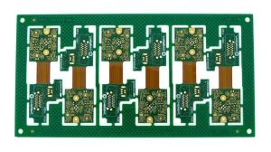
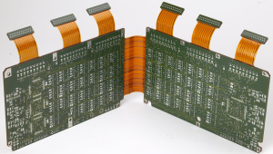
Rigid-Flex PCB Design
Rigid-flex boards combine rigid and flexible sections to reduce connectors, save space, and improve mechanical integration.
Controlled-Impedance PCB Design
Controlled impedance is essential for many high-speed and RF interfaces. Trace width, copper thickness, dielectric thickness, material properties, and stackup configuration must be considered together.
Common PCB Design Mistakes That Increase Costs
Choosing a PCB design partner with insufficient engineering experience can result in avoidable problems.
Common examples include:
- Poor component placement
- Excessively long signal paths
- Broken return-current paths
- Incorrect differential-pair routing
- Inadequate power-plane design
- Poor decoupling capacitor placement
- Insufficient thermal management
- Inadequate copper-to-edge clearance
- Insufficient annular rings
- Incorrect via structures
- Poor DFM integration
- Inadequate EMC considerations
- Missing production documentation
These issues may not become apparent until prototype fabrication, assembly, testing, or compliance certification.
The earlier they are identified, the lower the cost of correcting them.
Final Thoughts
Selecting the right PCB design company can have a major impact on product performance, manufacturing efficiency, reliability, and time to market.
A qualified PCB engineering partner should do more than create traces and generate Gerber files. The right partner should understand signal integrity, power integrity, controlled impedance, EMC/EMI, thermal management, DFM, assembly requirements, testing, and production engineering.
When evaluating PCB design companies, consider technical capabilities, relevant industry experience, certifications, communication processes, design-file ownership, DFM methodology, prototyping capabilities, and manufacturing support.
For complex projects involving high-speed, HDI, RF, multilayer, rigid-flex, medical, automotive, aerospace, or industrial electronics, selecting an experienced PCB design partner at the beginning of the project can significantly reduce engineering risk and unnecessary redesigns.
Looking for a Reliable PCB Design Partner?
Kingda provides professional PCB design services, PCB layout, DFM engineering, prototyping, PCB manufacturing, and PCB assembly support for a wide range of electronic products.
Our engineering team can support projects from schematic review and component placement through multilayer PCB layout, high-speed routing, impedance control, DFM verification, prototype development, and production preparation.
Whether you need a conventional multilayer PCB, HDI PCB, high-speed circuit board, RF PCB, or customized PCB solution, Kingda can help transform your electronic concept into a production-ready design.
Contact Kingda today to discuss your PCB design requirements and request a customized engineering solution.