PCB Panelization for SMT Assembly: Complete Design Guide
In modern electronics manufacturing, PCB panelization is widely used to improve production efficiency, reduce handling time, and optimize manufacturing costs. Instead of processing every individual printed circuit board separately, multiple PCB units can be combined into a larger manufacturing panel and processed together during SMT assembly.
For manufacturers and engineers, a properly designed panelized PCB can improve machine utilization, simplify component placement, reduce repeated setup operations, and provide more consistent production results.
This guide explains the major panelization methods, recommended design practices, manufacturing considerations, and common mistakes to avoid when preparing a PCB panel for SMT production.
What Is PCB Panelization?
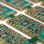
PCB panelization is the process of combining multiple individual PCB designs into one larger manufacturing panel. The individual boards remain connected during PCB fabrication and SMT assembly and are separated after production.
Panelization is particularly useful when a single PCB is relatively small. Processing several small boards together allows automated SMT equipment to handle a larger and more stable production panel instead of repeatedly loading and positioning individual boards.
A typical panel may include:
- Multiple identical PCB units
- Different PCB designs in the same panel
- Tooling rails
- Fiducial marks
- Tooling holes
- Breakaway tabs or V-grooves
- Manufacturing reference features
For customers using professional PCB assembly services, panel design should be considered together with PCB fabrication, stencil design, SMT placement, inspection, and depanelization.
Why Is PCB Panelization Important for SMT Assembly?
The main purpose of panelization is to make automated production more efficient.
During SMT assembly, PCB panels can reduce the number of times a production line needs to load, position, and process individual boards. This can shorten machine setup time and improve overall throughput.
Higher Production Efficiency
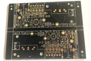
When several boards are processed as one panel, SMT equipment can place components across multiple PCB units during a single production cycle. This reduces repeated loading and unloading operations.
For prototype and low-volume production, panelization can also make small boards easier to handle on automated assembly equipment.
Lower Manufacturing Cost
Processing multiple boards together can reduce setup and handling costs. It may also improve material utilization during PCB fabrication.
For higher production volumes, these savings can become significant because the same manufacturing operations are repeated across many individual boards.
Improved Assembly Stability
Small PCBs can sometimes be difficult to transport through SMT equipment, particularly when they are thin, narrow, or irregularly shaped. Combining them into a larger panel provides greater mechanical stability during printing, placement, and reflow.
This is particularly important for flexible or thin PCB designs.
Common PCB Panelization Methods
Different panelization methods can be selected according to PCB geometry, material, thickness, component placement, and depanelization requirements.
The three common approaches are V-scoring, tab routing, and perforated breakaway tabs.
V-Scoring
V-scoring creates controlled grooves along the boundaries between individual PCB units.
The PCB remains mechanically connected during manufacturing but can be separated after assembly by applying mechanical force or using a depanelization machine.
V-scoring is generally suitable for rectangular or straight-edged PCB designs.
Advantages include:
- Simple panel construction
- Relatively clean separation
- Efficient use of PCB material
- Suitable for many standard rectangular boards
However, V-scoring is less suitable for boards with curved edges, internal cutouts, or highly irregular geometries.
Tab Routing
Tab routing uses small connection points to hold individual PCBs together.
This approach is more flexible than V-scoring and can accommodate irregular board shapes. The tabs can be positioned strategically to maintain sufficient mechanical strength throughout PCB fabrication and SMT processing.
After assembly, the boards are separated by cutting or breaking the remaining tabs.
Tab routing is particularly useful for panelized PCB designs containing curved, circular, or irregular outlines.
Perforated Breakaway Tabs
Perforated tabs use a series of small drilled holes to create a controlled breakaway area between PCB units.
This method can provide greater flexibility for unusual PCB geometries. However, engineers should consider the remaining rough edge after separation and whether it is acceptable for the final product.
For precision products, the depanelization method should be evaluated during the PCB design stage rather than after manufacturing.
PCB Panelization Design Rules
Good panelization is not simply about placing multiple boards next to each other. The panel must also provide sufficient space and reference features for PCB fabrication and SMT equipment.
Maintain Adequate Spacing Between Boards
A controlled gap should be maintained between individual PCB units.
The exact spacing depends on PCB geometry, fabrication method, tooling requirements, and the selected assembly process. In many practical designs, a small manufacturing gap is used between boards, while additional clearance may be required for special components or mechanical structures.
For flexible PCBs, additional spacing may be necessary to accommodate reinforcement materials and prevent mechanical interference.
Add Tooling Rails When Necessary
Tooling rails provide additional space around the panel and make it easier for automated equipment to transport and position the PCB.
A typical panel may require rails along one or more edges depending on the assembly line configuration.
Tooling rails can also provide space for:
- Tooling holes
- Fiducial marks
- Board identification
- Process reference information
- Edge clearance for components
The final rail dimensions should be confirmed with the PCB assembly manufacturer before production.
Use Fiducial Marks
Fiducial marks are reference points used by SMT machines and inspection systems to accurately determine PCB position and orientation.
A panel normally includes global fiducials, while individual PCB units may also require local fiducials for high-density or fine-pitch components.
Fiducial marks should remain clear of copper, solder mask openings, silkscreen, and other features that could interfere with machine vision.
Consider Component Clearance From the PCB Edge
Components located too close to the PCB edge may interfere with conveyors, tooling, depanelization equipment, or neighboring boards.
When designing a PCB panelization layout, engineers should check the distance between components and the board outline.
Extra attention should be given to:
- Large connectors
- Tall components
- Heavy components
- Edge-mounted components
- BGA and QFN packages
- Components extending beyond the PCB edge
If edge clearance is insufficient, additional tooling rails or a modified panel arrangement may be required.
Panel Size and SMT Equipment Compatibility
The final panel dimensions should be compatible with the PCB fabrication and SMT equipment used for production.
A panel that is too small may not provide enough area for stable automated handling. Conversely, an excessively large or heavy panel may create problems during transportation, solder paste printing, component placement, or reflow.
The appropriate panel size depends on:
- PCB dimensions
- PCB thickness
- Board material
- Component density
- SMT equipment
- Conveyor specifications
- Stencil dimensions
- Depanelization method
Therefore, panel dimensions should always be confirmed against the manufacturer’s current production capabilities.
Keep PCB Orientation Consistent
Whenever possible, individual PCB units should be arranged in the same orientation.
Consistent orientation simplifies SMT programming and reduces the possibility of incorrect component placement.
However, special situations may justify rotating or mirroring individual boards. For example, an engineer may use an optimized arrangement to improve material utilization or accommodate different component locations.
Before using such arrangements, verify that the orientation does not create assembly, inspection, or component-access problems.
Mixed PCB Panelization
Not every production panel needs to contain identical boards.
For some projects, different PCB designs can be combined into a single panel. This approach can be useful for prototype development, small-batch production, or products containing multiple related circuit boards.
However, mixed panelization requires careful control of:
- PCB dimensions
- Component heights
- Assembly orientation
- Fiducial locations
- SMT programming
- Quantity of each PCB type
- Depanelization requirements
When different PCB designs are assembled together, the production engineer should verify that every board can safely pass through the same printing, placement, reflow, and inspection process.
PCB Panelization for Flexible PCBs
Flexible PCB panelization requires additional mechanical considerations because FPC materials behave differently from rigid FR-4 boards.
Flexible boards can deform during handling, especially when they are thin or include heavy reinforcement components.
For FPC production, engineers should consider:
- Flexible material thickness
- Reinforcement areas
- Connection tabs
- Panel rigidity
- Component weight
- Bending zones
- Depanelization stress
The panel should provide enough mechanical support to prevent deformation during SMT production.
PCB Panelization and Stencil Design
Panelization directly affects stencil manufacturing.
The stencil opening pattern must correspond to the complete panel layout, including every PCB unit that will receive SMT components.
Before ordering a stencil, engineers should verify:
- PCB panel revision
- Component placement data
- Board orientation
- Fiducial locations
- Paste aperture design
- Panel dimensions
- Tooling requirements
The PCB, stencil, and SMT placement program should all be based on the same final production data.
This helps prevent mismatches between the physical panel and assembly files.
PCB Panelization and Quality Control
Panelization should also be considered from the perspective of inspection and testing.
A well-designed panel provides consistent positioning for SPI, AOI, X-ray inspection, and other quality-control processes.
Professional PCB manufacturing and assembly should include engineering verification before mass production to identify potential issues related to component clearance, panel strength, soldering, and testing.
Common PCB Panelization Mistakes to Avoid
Several panelization problems can increase manufacturing costs or create assembly defects.
Insufficient Board Spacing
Boards placed too close together may interfere with routing, depanelization, or components positioned near the edge.
Missing Fiducial Marks
Without appropriate fiducials, SMT equipment may have difficulty achieving accurate board positioning, particularly for high-density designs.
Oversized or Undersized Panels
Panels outside the recommended equipment range can create handling and production problems.
Poor Tab Placement
Too few tabs can cause the panel to flex during assembly, while excessive tabs can make depanelization unnecessarily difficult.
Ignoring Component Height
Tall components can interfere with adjacent PCB units or tooling rails and should be considered during panel layout.
Mixing Incompatible PCB Designs
Different boards may require different soldering profiles, assembly orientations, or inspection settings. Combining incompatible designs into one panel can complicate production.
Designing the Panel Too Late
Panelization should ideally be considered before PCB fabrication and SMT programming. Making panel changes after production preparation has started can result in additional engineering work and material costs.
How to Prepare a PCB Panel for Production

A practical panelization workflow can be organized into several stages.
Step 1: Review the PCB Design
Check the PCB outline, dimensions, thickness, component locations, and edge clearances.
Step 2: Select the Panelization Method
Choose V-scoring, tab routing, perforated tabs, or another appropriate method based on the board geometry.
Step 3: Determine Panel Arrangement
Optimize the number of boards per panel while maintaining sufficient manufacturing clearance.
Step 4: Add Tooling Features
Add tooling rails, tooling holes, fiducials, and other production references as required.
Step 5: Verify SMT Compatibility
Confirm that the panel can be processed by the intended solder paste printer, pick-and-place equipment, reflow oven, AOI, and other production equipment.
Step 6: Review Depanelization
Make sure the selected separation method will not damage components, solder joints, PCB edges, or sensitive areas.
Step 7: Final Engineering Review
Verify the PCB, Gerber files, BOM, pick-and-place data, stencil data, and panel design before releasing the project to manufacturing.
For turnkey production, component sourcing and engineering review can also be coordinated with the assembly process.
PCB Panelization vs. Individual PCB Processing
Processing individual boards may be suitable for very large PCBs or products with special mechanical requirements. However, PCB panelization is often more efficient when multiple small or medium-sized boards must be manufactured and assembled.
Panelization can provide:
- Higher SMT throughput
- Reduced handling operations
- Better production consistency
- Improved equipment utilization
- Lower setup costs
- More efficient manufacturing
The best approach depends on PCB geometry, order volume, assembly technology, and equipment limitations.
Final Checklist for PCB Panelization
Before releasing a panelized design to production, verify the following:
- Board spacing is consistent.
- Panel dimensions meet manufacturing requirements.
- Tooling rails are sufficient.
- Fiducial marks are correctly positioned.
- Tooling holes are available where required.
- Components have adequate edge clearance.
- Board orientation is correct.
- Tabs or V-grooves are suitable for the PCB geometry.
- Panel strength is sufficient for SMT processing.
- Stencil design matches the final panel.
- Pick-and-place data matches the panel orientation.
- Depanelization will not damage components or PCB edges.
- PCB, BOM, Gerber, and assembly files use the same revision.
Conclusion
A properly engineered PCB panelization strategy can significantly improve the efficiency and reliability of SMT assembly. By combining multiple boards into a production-ready panel, manufacturers can reduce handling operations, improve equipment utilization, simplify automated assembly, and optimize manufacturing costs.
The most important considerations include panel dimensions, board spacing, tooling rails, fiducial marks, component edge clearance, panel strength, depanelization method, stencil compatibility, and SMT equipment requirements.
For prototype, low-volume, and high-volume production, panel design should be reviewed together with PCB fabrication and assembly engineering rather than treated as a separate final-stage task.
A professional manufacturing partner can evaluate the panel design before production, identify potential DFM issues, and help ensure that the PCB, stencil, SMT program, inspection process, and depanelization method work together as one manufacturing system.
For projects requiring integrated PCB assembly, component procurement, SMT, THT, testing, and final integration, GOPCBA provides a one-stop electronics manufacturing solution designed to support projects from prototype through production. GOPCBA Official Website