How to Do PCB Panelization for SMT Assembly
In modern electronics manufacturing, PCB Panelization is widely used to improve production efficiency, simplify handling, and reduce manufacturing costs. Instead of processing individual circuit boards one at a time, multiple PCB units are arranged into a larger manufacturing panel and processed together.
For engineers and product designers, proper PCB Panelization Design is particularly important when preparing a board for automated SMT PCB Assembly. A well-designed panel can improve machine utilization, simplify component placement, reduce handling operations, and help maintain consistent assembly quality.
GOPCBA provides integrated PCB fabrication and assembly services, covering PCB manufacturing, SMT assembly, component sourcing, testing, and other electronics manufacturing processes.
What Is PCB Panelization?
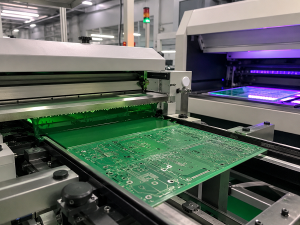
PCB Panelization is the process of combining multiple individual PCB designs into one larger production panel.
During PCB Assembly Manufacturing, automated equipment generally handles a panel more efficiently than very small individual boards. A panel allows several PCB units to pass through solder paste printing, component placement, reflow soldering, inspection, and other processes as a single manufacturing unit.
After assembly, the individual boards are separated from the panel using an appropriate depanelization method.
Why Is PCB Panelization Important?
Proper panelization can provide several benefits:
- Increase SMT production efficiency
- Reduce the number of times boards are loaded onto machines
- Improve board handling and transportation
- Support automated SMT placement
- Reduce production setup and handling costs
- Improve consistency between individual boards
- Make small or irregular PCBs easier to process
- Improve overall manufacturing throughput
For prototype and low-volume production, panelization can also make very small PCB designs easier to handle during automated assembly.
Common PCB Panelization Methods
The appropriate panelization method depends on the PCB outline, thickness, mechanical requirements, component placement, and depanelization process.
V-Cut Panelization
V-cut is one of the most common methods for rectangular PCB panels.
A V-shaped groove is partially cut along the boundary between individual boards. After PCB fabrication and assembly, the boards can be separated along the predefined groove.
V-cut panelization is particularly suitable for:
- Rectangular PCBs
- Boards with straight edges
- Repetitive PCB designs
- High-volume production
- Automated SMT PCB Assembly
However, V-cut is not ideal for complex curved or irregular PCB outlines because the cutting path must remain relatively straight.
Tab-Routed or Breakaway Panelization
Tab routing uses small connecting tabs to join individual PCB units together.
This method provides greater flexibility than V-cut and can be used for boards with irregular outlines, curves, slots, or other complex shapes.
The connecting tabs should be positioned carefully to provide sufficient mechanical support while allowing clean separation after assembly.
For flexible circuits, the panel design should be evaluated separately because the mechanical behavior of flexible materials differs significantly from rigid PCBs.
Mixed or Special Panelization
Some projects require more advanced configurations, such as:
- Different PCB designs on one panel
- Mirrored PCB arrangements
- Mixed board sizes
- Irregular PCB shapes
- Top-side and bottom-side combinations
- Special mechanical support structures
These configurations require careful engineering review because component interference, assembly orientation, tooling access, and depanelization must all be considered.
PCB Panelization Design Guidelines
A successful PCB Panelization Design should consider both PCB fabrication and downstream assembly requirements.
1. Maintain Consistent Board Spacing
A small gap should normally be maintained between individual PCB units.
The exact spacing depends on the PCB manufacturer, board material, panel structure, and depanelization method. A practical engineering approach is to maintain a consistent gap across the entire panel and confirm the final value with the manufacturer before production.
For flexible PCB assemblies or boards with stiffeners, additional spacing may be necessary to prevent mechanical interference.
2. Add Tooling Edges When Required
Tooling edges provide additional support for automated assembly equipment.
They can be particularly useful when:
- Components are close to the PCB edge
- The PCB is too small for stable machine handling
- The board requires SMT fiducial marks
- The board needs additional mechanical support
- The assembly process requires conveyor or clamping clearance
A typical panel may include tooling rails along one or more sides of the panel.
The tooling-edge width should be determined according to the assembly equipment and PCB manufacturer’s process requirements rather than treated as a universal value.
3. Add Tooling Holes
Tooling holes help equipment accurately position and secure the panel during manufacturing.
They should be:
- Located consistently
- Mechanically stable
- Clear of copper and components where required
- Positioned according to the assembly equipment
- Designed with sufficient clearance from other features
If the PCB is used for automated PCB Assembly, tooling holes should be included in the panel design whenever they are required by the manufacturing process.
4. Use Fiducial Marks
Fiducial marks provide optical reference points for automated SMT equipment.
A machine can use these reference points to determine the precise position and orientation of the PCB or panel before component placement.
Fiducials are especially important for high-density assemblies, fine-pitch components, BGA packages, and other precision SMT PCB Assembly applications.
When designing fiducials, avoid placing copper, solder mask openings, components, or other visual interference too close to the fiducial area.
Recommended PCB Panel Dimensions
The optimum panel size depends on the capabilities of the SMT line, PCB fabrication equipment, conveyor system, board thickness, and component distribution.
There is no universal panel dimension that is appropriate for every project.
When selecting a panel size, consider:
- PCB dimensions
- Number of boards per panel
- Board thickness
- Component height
- Component weight
- SMT equipment limitations
- Conveyor width
- Depanelization method
- Warpage risk
- Tooling requirements
For very small PCBs, panelization can be especially useful because individual boards may be difficult for automated equipment to transport and process reliably.
For large panels, however, excessive panel size can increase mechanical stress and the risk of PCB warpage.
Component Placement Near the PCB Edge
Component-to-edge clearance is one of the most important considerations in PCB Panelization Design.
Components positioned too close to the board edge may interfere with:
- SMT machine tooling
- Conveyors
- Clamping mechanisms
- V-cut operations
- Routing tools
- Depanelization equipment
Sensitive components should therefore be kept away from panel separation lines whenever possible.
If edge-mounted components are unavoidable, additional engineering measures may be required, such as tooling rails, special routing, or alternative depanelization methods.
PCB Orientation and Panel Arrangement
Individual PCB units should generally be arranged in the same orientation.
Consistent orientation simplifies automated production and reduces the possibility of incorrect component placement or process setup.
However, special arrangements may sometimes be necessary to maximize material utilization or avoid component interference.
Examples include:
- Mirrored panels
- Alternating board orientation
- Top/bottom combinations
- Different PCB designs on the same panel
These configurations should be reviewed carefully before production.
Panelization for Flexible PCBs
Flexible PCB panelization requires additional mechanical considerations.
FPCs are thinner and more flexible than rigid PCBs, so excessive panel size, insufficient support, or heavy components can cause deformation during assembly.
For FPC applications, engineers should pay particular attention to:
- Connecting tabs
- Stiffener locations
- Panel spacing
- Board orientation
- Component weight
- Mechanical support
- Separation method
Unlike rigid PCBs, flexible circuits may not be suitable for conventional V-cut processing. The panelization method should therefore be selected according to the FPC construction and manufacturing process.
How PCB Panelization Improves SMT Manufacturing
The primary purpose of PCB Panelization is to make automated production more efficient.
A properly designed panel allows several boards to be processed together through the same manufacturing sequence:
PCB Fabrication → Solder Paste Printing → SMT Placement → Reflow Soldering → AOI → X-Ray/Testing → Depanelization → Final Inspection
Modern SMT PCB Assembly facilities can combine automated placement equipment with solder paste inspection, AOI, X-ray inspection, and electrical testing to improve manufacturing consistency. GOPCBA’s published capabilities include SMT assembly, AOI, X-ray, ICT/FCT, and other inspection and testing processes.
When Should You Panelize a PCB?
Panelization is particularly useful when:
Small PCB Size
Very small boards can be difficult to handle individually. Combining multiple units into a larger panel provides better mechanical support for automated assembly.
High Production Quantities
For medium- and high-volume manufacturing, panelization can improve equipment utilization and reduce repetitive machine loading operations.
Prototype and Low-Volume Production
Panelization can also be useful for prototypes when individual boards are too small for efficient automated processing.
GOPCBA supports PCB assembly from prototypes and low-volume production through higher-volume manufacturing, making panelization applicable across different stages of product development.
PCB Panelization Checklist
Before releasing a panelized PCB for PCB Assembly Manufacturing, review the following items:
- Confirm the final panel dimensions
- Verify the spacing between individual boards
- Select an appropriate V-cut or tab-routing method
- Check component-to-edge clearance
- Add tooling edges when necessary
- Add tooling holes when required
- Add appropriate fiducial marks
- Confirm PCB orientation
- Check component interference
- Consider PCB thickness and panel rigidity
- Evaluate potential board warpage
- Confirm the depanelization method
- Verify that the panel is compatible with the SMT production line
- Review the final manufacturing drawing before production
PCB Panelization Best Practices
The best panel design is not simply the one that fits the largest number of PCBs onto a sheet. It should balance material utilization, assembly efficiency, mechanical stability, inspection requirements, and depanelization quality.
A good PCB Panelization Design should therefore follow these principles:
- Keep the panel structure symmetrical where practical.
- Maintain consistent spacing between PCB units.
- Avoid placing sensitive components near separation lines.
- Provide sufficient support for thin or flexible boards.
- Use fiducial marks for automated optical alignment.
- Add tooling edges when required by the assembly process.
- Avoid excessive panel dimensions that may increase warpage.
- Select the separation method according to the PCB outline.
- Review panelization together with the SMT manufacturing process.
- Confirm the final panel design with the PCB and assembly manufacturer before production.
PCB Panelization and One-Stop PCB Assembly
Panelization is only one part of the overall electronics manufacturing process. For complex projects, coordinating PCB fabrication, component sourcing, SMT assembly, testing, and final delivery through a single manufacturing partner can simplify production management.
GOPCBA provides integrated PCB manufacturing and assembly services covering PCB fabrication, component procurement, SMT, THT, testing, and other PCBA manufacturing requirements.
One-Stop PCBA Manufacturing Services
Final Thoughts
Proper PCB Panelization can significantly improve the efficiency and reliability of automated electronics manufacturing. By selecting the right panel structure, maintaining appropriate board spacing, adding tooling features, using fiducial marks, and considering component placement and depanelization requirements, engineers can create panels that are easier to fabricate and assemble.
The most important point is that panelization should be designed together with the complete manufacturing process—not treated as an isolated PCB layout task. When PCB fabrication and SMT PCB Assembly requirements are considered from the beginning, the resulting panel can provide better production efficiency, improved handling, and more consistent assembly quality.
For projects ranging from prototypes to volume production, working with an experienced PCB Assembly manufacturer can also help identify panelization issues before manufacturing begins.