PCB Stencil: Types, Materials, Manufacturing Process, Design Guidelines, and Applications
As PCB manufacturing technology continues to evolve, Surface Mount Technology (SMT) has become one of the most important production methods for manufacturing compact, high-density, and reliable electronic assemblies. SMT enables manufacturers to place a large number of electronic components on relatively small circuit boards while maintaining high production efficiency and assembly accuracy.
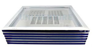
One of the most important steps in the SMT process is solder paste printing, and the PCB stencil is the critical tool that makes accurate solder paste deposition possible. A properly designed stencil transfers a controlled amount of solder paste onto specific PCB pads, creating the foundation for reliable solder joints during reflow soldering.
Although a PCB stencil may look like a simple thin metal sheet, its material, thickness, aperture geometry, surface finish, alignment accuracy, and manufacturing quality can have a significant impact on SMT assembly quality.
This guide explains what a PCB stencil is, how it works, the major types and materials, the manufacturing process, essential design considerations, common printing defects, applications, and how to choose a reliable PCB stencil manufacturer.
What Is a PCB Stencil?
A PCB stencil, also known as an SMT stencil or solder paste stencil, is a thin sheet of material containing precisely positioned openings called apertures. These apertures correspond to selected solder pads on a PCB and allow a controlled amount of solder paste to be deposited during the SMT printing process.
Most high-quality PCB stencils are manufactured from stainless steel because it provides excellent dimensional stability, mechanical strength, durability, and resistance to chemical cleaning agents.
During SMT assembly, the stencil is aligned with the PCB, and solder paste is applied across its surface using a squeegee. The solder paste passes through the stencil apertures and is deposited onto the corresponding PCB pads.
After the stencil is separated from the PCB, the deposited solder paste remains on the pads. Pick-and-place equipment then positions the SMD components onto the solder paste deposits, followed by reflow soldering.
Without an accurately manufactured stencil, achieving consistent solder paste volume and precise deposition becomes extremely difficult, particularly for high-density PCBs, fine-pitch components, QFNs, BGAs, and other miniature packages.
A high-quality stencil therefore plays an important role in controlling:
- Solder paste volume
- Solder paste placement accuracy
- Solder joint consistency
- Component placement quality
- Solder bridging
- Tombstoning
- Voiding
- Overall SMT assembly yield
How Does a PCB Stencil Work?
The basic function of a PCB stencil is straightforward: it selectively transfers solder paste from the stencil surface to designated PCB pads.
However, the actual SMT printing process involves several carefully controlled steps.
1. PCB and Stencil Alignment
The bare PCB or PCB panel is positioned on the SMT production line. The stencil is then placed above the PCB and aligned according to the board’s fiducial marks and tooling system.
For panelized PCB production, the stencil is designed according to the complete panel layout rather than an individual board.
Modern stencil printers commonly use automated vision systems to identify fiducials and compensate for minor positioning variations. Accurate alignment is essential because even a small offset can result in incomplete pad coverage or excessive solder paste on adjacent pads.
2. Solder Paste Application
Solder paste consists primarily of solder alloy particles suspended in a flux medium. The solder paste is placed on the stencil surface, and a squeegee moves across the stencil with controlled pressure and speed.
As the squeegee travels across the stencil, solder paste fills the apertures and transfers onto the PCB pads.
The amount of solder paste deposited depends on several factors, including:
- Stencil thickness
- Aperture dimensions
- Aperture geometry
- Squeegee pressure
- Printing speed
- Separation speed
- Solder paste characteristics
- PCB surface condition
The goal is not simply to deposit as much solder paste as possible. The objective is to achieve the correct solder paste volume for each component.
3. Stencil Separation
After printing, the stencil is separated from the PCB. This process is often referred to as stencil release or snap-off.
The solder paste must release cleanly from the aperture walls and remain on the PCB pad. Poor release can produce insufficient solder paste deposits, inconsistent volumes, or distorted deposits.
A well-designed stencil therefore requires suitable aperture dimensions, appropriate thickness, smooth aperture walls, and proper printing parameters.
4. Inspection
After solder paste printing, the PCB is typically inspected using a solder paste inspection (SPI) system.
SPI equipment can measure parameters such as:
- Paste volume
- Paste height
- Paste area
- Paste position
- Deposit shape
If abnormalities are detected, the printing process can be adjusted before large quantities of defective boards are produced.
The stencil itself should also be inspected and cleaned regularly to prevent solder paste accumulation around apertures.
Types of PCB Stencils
Different PCB assembly requirements call for different stencil configurations. The most common categories include framed stencils and frameless stencils.
1. Framed PCB Stencils
A framed stencil consists of a thin metal stencil foil permanently mounted inside a rigid frame, usually made from aluminum.
The stencil foil is typically manufactured from stainless steel and contains laser-cut apertures corresponding to the PCB pad layout.
Framed stencils are widely used in automated SMT production because the rigid frame provides excellent stability and repeatable positioning.
Advantages:
- Excellent dimensional stability
- High printing repeatability
- Suitable for high-volume production
- Fast installation on automated stencil printers
- Long service life when properly maintained
Disadvantages:
- Higher manufacturing cost
- Requires more storage space
- More difficult to transport
- Each stencil generally requires its own frame
2. Frameless PCB Stencils
A frameless stencil is a stencil foil without a permanent rigid frame. During printing, the foil is installed into a reusable tensioning frame or stencil tensioning system.
Frameless stencils are particularly useful for prototypes, low-volume production, engineering development, and applications where multiple stencil designs need to share the same reusable frame.
Advantages:
- Lower initial cost
- Easier to store and transport
- Reduced material consumption
- Reusable frame systems can support multiple stencil foils
- Suitable for prototypes and smaller production runs
Disadvantages:
- Requires an appropriate tensioning system
- Setup can take longer
- Printing consistency depends heavily on stencil tension
- Generally less convenient than framed stencils for some high-volume automated applications
Materials Used for PCB Stencils
Material selection directly influences stencil durability, dimensional stability, aperture quality, solder paste release, and manufacturing cost.
The most commonly used materials include stainless steel, nickel, and polymer-based materials.
Stainless Steel
Stainless steel is the most widely used material for modern PCB stencil manufacturing.
It provides an excellent combination of strength, rigidity, corrosion resistance, dimensional stability, and durability.
High-quality stainless steel stencils are particularly suitable for fine-pitch SMT assembly and high-volume manufacturing.
Advantages:
- High mechanical strength
- Excellent dimensional stability
- Good wear resistance
- Long service life
- Suitable for fine-pitch applications
- Compatible with automated SMT printing equipment
Potential limitations:
- Higher weight than polymer stencils
- Requires appropriate cleaning and handling
- Surface condition can affect solder paste release
Nickel
Nickel stencils are commonly manufactured through an electroforming process rather than conventional laser cutting.
Electroformed nickel can provide extremely smooth aperture walls, which may improve solder paste release for demanding fine-pitch applications.
Advantages:
- Smooth aperture walls
- Excellent solder paste release
- High dimensional precision
- Suitable for ultra-fine-pitch applications
- Useful for demanding miniature components
Potential limitations:
- Higher manufacturing cost
- Longer manufacturing process
- Requires specialized electroforming technology
Polymer Materials
Polyester and polyimide are examples of polymer materials that can be used for certain stencil applications.
Polymer stencils are generally intended for prototypes, temporary production, low-volume projects, or applications where cost and flexibility are more important than maximum durability.
Advantages:
- Low cost
- Lightweight
- Easy to store
- Fast to manufacture
- Convenient for prototyping and design iterations
Disadvantages:
- Lower dimensional stability
- Lower mechanical durability
- Limited service life
- Generally unsuitable for demanding high-volume fine-pitch production
PCB Stencil Manufacturing Process
The PCB stencil manufacturing process requires high dimensional accuracy because even small variations in aperture dimensions can affect solder paste volume and SMT assembly quality.
The main manufacturing steps include design preparation, material preparation, aperture formation, finishing, inspection, and final validation.
1. Design and Data Preparation
The process begins with PCB design data, typically supplied in Gerber or other compatible manufacturing formats.
The manufacturer analyzes:
- PCB dimensions
- Pad locations
- Component footprints
- Fiducial marks
- Panelization
- Aperture dimensions
- Stencil thickness
- Special component requirements
A professional PCB stencil manufacturer should also perform a design-for-manufacturing review before fabrication.
This step helps identify potential problems with fine-pitch pads, thermal pads, BGA footprints, insufficient spacing, and other challenging areas.
2. Material Preparation
The appropriate stencil material and thickness are selected based on the PCB design and assembly requirements.
For example, stainless steel may be selected for general SMT production, while specialized nickel stencils may be considered for demanding fine-pitch applications.
3. Aperture Formation
Laser cutting is one of the most common methods for producing stainless steel stencil apertures.
A high-precision laser creates the required openings according to the digital stencil design.
The process must control:
- Aperture size
- Aperture shape
- Position accuracy
- Taper
- Edge quality
- Wall smoothness
For electroformed nickel stencils, a different manufacturing method is used. A photolithographic pattern is created on a mandrel, after which nickel is electroformed to the required thickness before the stencil is separated from the mandrel.
4. Surface Finishing
Depending on the application, additional finishing processes may be applied to improve stencil performance.
These can include polishing, electropolishing, nano-coating, or other surface treatments.
The objective is to improve aperture smoothness and solder paste release while reducing paste adhesion.
5. Frame Assembly
For framed stencils, the stencil foil is mounted into a rigid frame under controlled tension.
Correct tension is essential because insufficient or uneven tension can affect stencil-to-PCB contact and printing repeatability.
6. Inspection and Validation
The completed stencil should undergo dimensional and visual inspection.
Important inspection items include:
- Aperture dimensions
- Aperture position
- Stencil thickness
- Frame dimensions
- Tension
- Surface condition
- Burrs and contamination
- Fiducial alignment
For demanding applications, manufacturers may use automated optical inspection or precision measurement equipment to verify the stencil against the original design data.
PCB Stencil Design Considerations
Proper PCB stencil design is one of the most important factors affecting solder paste printing quality.
The stencil should not simply reproduce every PCB pad at a 1:1 ratio. Apertures often need to be modified according to component type, pad geometry, pitch, thermal requirements, and solder paste behavior.
Aperture Design
Aperture geometry determines how solder paste enters and exits the stencil.
Common aperture shapes include:
- Square
- Rectangular
- Circular
- Rounded rectangle
- Home-plate
- Window-pane
- Modified trapezoidal designs
For fine-pitch components, aperture dimensions may be reduced or modified to minimize solder bridging.
For large exposed thermal pads, window-pane or segmented apertures can help control solder paste volume and reduce voiding.
For BGA and fine-pitch applications, aperture dimensions must be carefully optimized according to ball size, pad diameter, pitch, stencil thickness, and solder paste characteristics.
Area Ratio
The area ratio is an important parameter in stencil design because it influences solder paste release from an aperture.
For a typical rectangular aperture, the area ratio can be expressed as:
Area Ratio = Aperture Area / Aperture Wall Area
For a rectangular aperture:
Area Ratio = (L × W) / [2 × (L + W) × T]
where:
- L = aperture length
- W = aperture width
- T = stencil thickness
As a general guideline, an area ratio of approximately 0.66 or higher is often targeted for reliable solder paste release, although the appropriate value depends on the specific stencil, solder paste, component geometry, and printing process.
Aspect Ratio
Aspect ratio compares the aperture width with the stencil thickness.
For a rectangular aperture:
Aspect Ratio = Aperture Width / Stencil Thickness
An aspect ratio above approximately 1.5 is commonly used as a general design guideline for reliable solder paste release.
However, area ratio is often a more useful parameter when evaluating modern fine-pitch stencil designs.
Stencil Thickness
Stencil thickness directly affects the amount of solder paste deposited onto the PCB.
Typical stencil thicknesses may range from approximately 3 mil (0.076 mm) to 8 mil (0.203 mm), depending on the component mix and application.
Thicker stencils can provide more solder paste for larger components, while thinner stencils are generally better suited for fine-pitch components.
For mixed-technology assemblies, a stepped stencil may be considered.
Step Stencils
Step stencils incorporate different thicknesses in different areas of the same stencil.
For example, a thinner region can support fine-pitch components while a thicker region provides sufficient solder paste volume for larger components.
Step stencils are useful for complex PCB assemblies containing both miniature and large components.
Benefits of Using a High-Quality PCB Stencil
A properly manufactured stencil can provide significant advantages throughout the SMT assembly process.
1. Accurate Solder Paste Deposition
A high-quality stencil ensures that the correct amount of solder paste is deposited at the correct location.
This helps reduce:
- Solder bridges
- Insufficient solder
- Open joints
- Tombstoning
- Component displacement
- Excessive solder volume
2. Support for Advanced PCB Assembly
Modern electronic products often contain fine-pitch components, BGAs, QFNs, micro-BGAs, and other high-density packages.
A precision stencil enables manufacturers to achieve the controlled solder paste deposition required by these advanced assemblies.
This is particularly important for:
- HDI PCB
- Automotive electronics
- Medical electronics
- Aerospace electronics
- Industrial control systems
- Power electronics
- Communication equipment
- Consumer electronics
3. Reduced Manufacturing Cost
Consistent solder paste deposition can reduce rework, scrap, component replacement, and production downtime.
Although a high-quality stencil may require a higher initial investment, improved process stability can significantly reduce total assembly costs over time.
4. Improved Production Repeatability
A well-designed stencil produces repeatable solder paste deposits across large production runs.
This consistency is particularly valuable in high-volume SMT production, where even a small process variation can result in significant numbers of defective assemblies.
Applications of PCB Stencils
PCB stencils are used throughout the electronics manufacturing industry wherever SMT components need to be assembled.
SMT PCB Assembly
The most common application is automated SMT assembly.
PCB stencils are used for:
- Consumer electronics
- Automotive electronics
- Medical devices
- Industrial equipment
- Telecommunications
- Power electronics
- Aerospace systems
- Defense electronics
- IoT devices
- Computer hardware
Adhesive Printing
In some SMT processes, stencil printing is used to deposit adhesive rather than solder paste.
The adhesive can help secure components to the PCB before subsequent soldering operations, particularly in specific assembly configurations.
PCB Rework and Repair
Custom stencils can also be used during PCB repair and rework.
A localized stencil can deposit solder paste only onto a specific area of the board, making it useful for replacing individual components or repairing selected PCB sections.
PCB Stencil Printing vs. PCB Screen Printing
PCB stencil printing and screen printing are related processes, but they serve different purposes.
PCB stencil printing is primarily used during SMT assembly to deposit solder paste onto specific PCB pads.
PCB screen printing, on the other hand, is commonly used to apply silkscreen ink to the PCB surface. This layer can include:
- Component reference designators
- Polarity indicators
- Logos
- Warning symbols
- Assembly instructions
- Other identifying marks
The two processes use different materials, designs, and process parameters.
As PCB components became smaller and SMT layouts became denser, metal stencils became increasingly important because they provide much greater control over solder paste volume and placement than traditional screen-based solder paste printing.
Common PCB Stencil Printing Challenges
Although stencil printing is highly automated, several problems can occur if the stencil design, equipment, materials, or process parameters are not properly controlled.
1. Stencil Misalignment
Stencil misalignment occurs when stencil apertures do not correctly match the PCB pads.
Common causes include:
- Incorrect stencil data
- Poor calibration
- Incorrect fiducial recognition
- PCB warpage
- Stencil deformation
- Improper tooling
Potential effects:
- Incomplete solder paste coverage
- Excessive solder paste deposition
- Component placement problems
- Solder bridging
- Open solder joints
2. Solder Bridging
Solder bridging occurs when solder connects two adjacent pads or component leads that should remain electrically isolated.
Common causes include:
- Apertures that are too large
- Insufficient pad spacing
- Excessive solder paste volume
- Poor stencil release
- Incorrect printing pressure
- Excessive paste accumulation
Potential effects:
- Electrical short circuits
- Reduced product reliability
- Functional failures
- Increased rework
3. Tombstoning
Tombstoning, also known as the Manhattan effect, occurs when one end of a small two-terminal component lifts away from the PCB pad during reflow.
It is particularly common with small passive components such as chip resistors and capacitors.
Potential causes include:
- Uneven solder paste deposition
- Unequal pad geometry
- Different thermal conditions
- Component placement variation
- Improper reflow profile
A well-designed stencil can help reduce tombstoning by ensuring more consistent solder paste volumes on both pads.
4. Insufficient Solder Paste
Insufficient solder paste can result from poor aperture design, inadequate paste release, stencil contamination, excessive printing speed, or incorrect stencil thickness.
The result may be weak solder joints, incomplete connections, or open circuits.
5. Excessive Solder Paste
Excessive solder paste can cause solder bridging, solder balls, component displacement, and other assembly defects.
Controlling stencil thickness and aperture dimensions is therefore essential.
6. Stencil Contamination
Solder paste can accumulate on the bottom side of a stencil after repeated printing cycles.
If the stencil is not cleaned properly, paste contamination can transfer to adjacent PCB areas and reduce printing accuracy.
Regular stencil cleaning is therefore an important part of SMT process control.
How to Choose a Reliable PCB Stencil Manufacturer
Selecting the right PCB stencil manufacturer can directly affect SMT assembly quality, production yield, and manufacturing cost.
Before selecting a supplier, manufacturers should evaluate technical capabilities, manufacturing accuracy, material quality, turnaround time, engineering support, and overall cost.
Design and Engineering Support
A professional stencil manufacturer should be able to review PCB design data and identify potential printing problems before manufacturing begins.
The supplier should understand:
- Fine-pitch components
- BGA packages
- QFN packages
- Thermal pads
- Mixed component sizes
- Step stencil requirements
- Area ratio
- Aspect ratio
- Aperture optimization
Engineering support is particularly important for complex or high-density PCB assemblies.
Manufacturing Quality
The supplier should use appropriate precision manufacturing equipment, such as high-accuracy laser cutting systems and advanced finishing technologies.
Important quality-control capabilities include:
- Precision aperture inspection
- Thickness measurement
- Dimensional inspection
- Tension testing
- Surface inspection
- Data-to-stencil verification
Material Selection
The manufacturer should provide suitable options such as stainless steel, nickel, or specialized polymer materials depending on the application.
For most production applications, stainless steel provides an excellent balance of performance, durability, and cost.
Cost and Quality
Stencil cost should not be evaluated based solely on the initial quotation.
A low-cost stencil with poor aperture accuracy may result in higher costs due to:
- Rework
- Scrap
- Production downtime
- Soldering defects
- Reduced assembly yield
A higher-quality stencil can therefore provide a lower total cost of ownership over its service life.
Delivery and Technical Support
Fast turnaround can be particularly important during prototype development and urgent production projects.
A reliable supplier should provide clear communication, accurate manufacturing schedules, technical support, and responsive after-sales service.
For companies requiring customized PCB stencil manufacturing, Kingda can provide engineering-oriented support for stencil design, SMT assembly requirements, and PCB production needs.
PCB Stencil Maintenance and Cleaning
Proper stencil maintenance is essential for maintaining consistent printing performance.
After repeated printing cycles, solder paste may accumulate around stencil apertures and on the underside of the foil.
Recommended maintenance practices include:
- Clean the stencil at appropriate intervals.
- Use compatible cleaning chemicals.
- Avoid damaging aperture walls.
- Inspect apertures regularly.
- Store stencils in a clean, dry environment.
- Protect the stencil from mechanical deformation.
- Verify stencil tension when applicable.
- Record maintenance and inspection results.
For high-volume production, a preventive maintenance schedule can help extend stencil service life and maintain printing consistency.
PCB Stencil Quality Control
Quality control should begin before stencil manufacturing and continue throughout its service life.
A comprehensive inspection program may include:
- Design verification
- Material verification
- Thickness inspection
- Aperture dimensional inspection
- Aperture position verification
- Surface inspection
- Frame and tension inspection
- Stencil-to-PCB alignment verification
- Solder paste printing validation
For advanced PCB assembly, SPI data can also be used to evaluate stencil performance and determine whether aperture modifications are required.
Conclusion
A PCB stencil is one of the most important tools in modern SMT assembly. Although it is essentially a thin sheet containing precisely engineered apertures, its design and manufacturing accuracy have a direct impact on solder paste deposition, solder joint quality, assembly yield, and overall PCB reliability.
The material, stencil thickness, aperture geometry, area ratio, aspect ratio, surface finish, tension, and alignment must all be carefully considered when designing a stencil.
For standard SMT production, stainless steel remains the most widely used stencil material because of its excellent strength, dimensional stability, durability, and printing performance. For demanding fine-pitch applications, specialized nickel stencils, advanced surface treatments, and optimized aperture designs can provide additional performance benefits.
As electronic products continue to become smaller, faster, and more densely integrated, SMT stencil technology is also evolving. Fine-pitch components, advanced semiconductor packages, HDI designs, miniaturized electronics, and high-reliability applications are driving demand for more precise stencil manufacturing.
Advanced laser cutting, electroforming, electropolishing, nano-coatings, automated inspection, and AI-assisted stencil optimization are expected to further improve solder paste transfer efficiency and manufacturing consistency.
For companies looking for dependable PCB stencil manufacturing, professional engineering support and strict quality control are just as important as the stencil itself. By working with an experienced supplier such as Kingda, manufacturers can optimize stencil design, improve solder paste printing quality, reduce assembly defects, and achieve more stable SMT production.