What Is a Quick-Turn PCB?
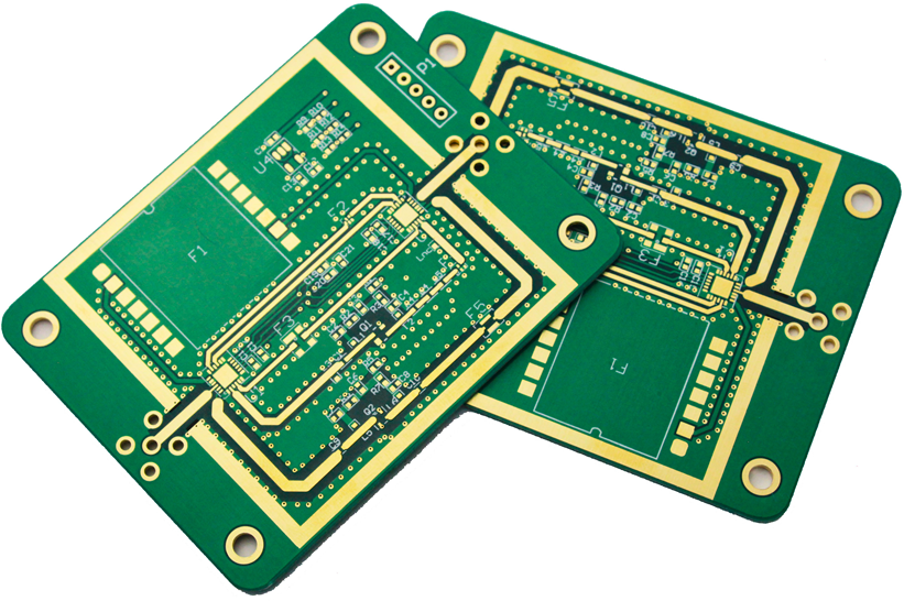
A quick-turn PCB is a printed circuit board manufactured and delivered through an accelerated production process. Compared with conventional PCB manufacturing, quick-turn services significantly reduce the time required to move from design files to finished circuit boards.
Quick-turn PCB manufacturing is particularly valuable when a product has a demanding development schedule, engineers need to validate a prototype quickly, or a production line requires an urgent replacement board. In these situations, even a few days of manufacturing delay can affect testing, product certification, system integration, and the overall product launch schedule.
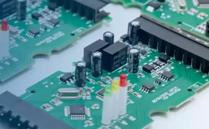
A conventional PCB production cycle may take several weeks depending on board complexity, material availability, order volume, and factory capacity. By contrast, quick-turn PCB manufacturing can often produce simple prototype boards within 24–48 hours, while more complex multilayer or HDI designs may require several additional days.
The exact lead time depends on factors such as:
- Board layer count
- PCB dimensions
- Material selection
- Copper thickness
- Minimum trace width and spacing
- Via structure
- Surface finish
- Impedance requirements
- HDI or microvia technology
- Order quantity
- Manufacturing capacity
- PCB assembly requirements
Importantly, fast production should not mean lower quality. A reputable PCB manufacturer should apply the same fundamental quality requirements to quick-turn and standard orders. The primary difference is how production resources are prioritized and scheduled.
Manufacturers can accelerate production by reserving commonly used materials, prioritizing urgent orders, optimizing production scheduling, operating multiple shifts, and maintaining dedicated capacity for prototype and expedited orders.
Quick-Turn PCB Manufacturing Process
The quick-turn PCB manufacturing process includes essentially the same core manufacturing stages used for standard PCB production. The primary difference is that engineering review, material preparation, production scheduling, and manufacturing operations are optimized to minimize idle time.
Step 1: Design File Review
The process begins when the customer submits PCB manufacturing data, typically including Gerber files or ODB++ files, drill files, board specifications, stack-up information, and other required documentation.
The manufacturer performs engineering review and Design for Manufacturability (DFM) analysis to identify potential problems before fabrication begins.
Typical checks include:
- Minimum trace width and spacing
- Hole diameter and aspect ratio
- Copper thickness
- Solder mask clearance
- Silkscreen clearance
- Board outline
- Layer registration
- Annular ring dimensions
- Impedance requirements
- Via structures
- Manufacturing tolerances
For quick-turn orders, fast engineering feedback is particularly important. Identifying a DFM problem before production prevents the order from being delayed by repeated file revisions.
Step 2: Material Selection and Preparation
Material availability is one of the most important factors affecting PCB lead time.
Manufacturers that provide quick-turn services generally maintain inventory of commonly used materials, such as standard FR-4 laminates and common copper foils.
For example, a conventional FR-4 PCB using standard copper thickness can usually be processed faster than a board requiring a specialized high-frequency laminate, unusual dielectric thickness, or non-standard copper construction.
For this reason, selecting standard materials whenever the application permits can significantly improve production speed.
Step 3: Inner-Layer Imaging
For multilayer PCBs, the inner copper layers are prepared and imaged according to the PCB layout.
Modern manufacturers may use Direct Laser Imaging (DLI) to transfer circuit patterns onto the copper surface. Because DLI can eliminate or reduce the need for conventional phototools, it can help shorten preparation time and improve registration accuracy.
After imaging, the copper pattern is developed and etched to create the required inner-layer circuitry.
Step 4: Lamination and CNC Drilling
Once the inner layers have been fabricated and inspected, the multilayer stack-up is assembled using copper foil, prepreg, and core materials.
The stack is laminated under controlled temperature and pressure to create a mechanically stable multilayer PCB structure.
After lamination, CNC drilling creates through-holes, vias, and other specified holes.
For high-priority production, manufacturers may operate multiple shifts or extended production schedules to minimize waiting time between processes.
Step 5: Copper Plating and Outer-Layer Circuit Formation
After drilling, the exposed hole walls require metallization so that electrical connections can be established between PCB layers.
A chemical copper deposition process creates a conductive layer inside the drilled holes. Additional copper plating can then build the required copper thickness.
The outer-layer circuitry is subsequently formed through imaging and etching processes.
Precise control of plating thickness, etching, registration, and line geometry is essential because these parameters directly affect electrical performance and long-term reliability.
Step 6: Solder Mask and Surface Finish
The PCB is then coated with solder mask to protect exposed copper and reduce the risk of solder bridges during assembly.
The manufacturer applies the selected surface finish according to the design requirements and intended application.
Common PCB surface finishes include:
- HASL
- Lead-free HASL
- ENIG
- OSP
- Immersion tin
- Immersion silver
ENIG PCB technology is frequently selected for prototype and high-reliability applications because it provides a relatively flat surface and good solderability. HASL remains a cost-effective option for many conventional PCB designs.
Step 7: Electrical Testing and Final Inspection
Quick-turn production should never eliminate essential quality-control procedures.
Depending on the PCB design and production requirements, inspection may include:
- Automated Optical Inspection (AOI)
- Electrical continuity testing
- Isolation testing
- Dimensional inspection
- Solder mask inspection
- Surface finish inspection
- Microsection analysis for selected production requirements
- Final visual inspection
The goal is to achieve faster delivery without compromising the electrical, mechanical, and manufacturing requirements of the PCB.
Typical Quick-Turn PCB Lead Times
Quick-turn PCB lead time refers to the amount of time required to manufacture and deliver the finished circuit boards.
Actual lead time varies according to board complexity and manufacturer capability, but common service levels include:
| Service Level | Typical Lead Time | Typical Application |
|---|---|---|
| Same-day / 24-hour | Up to 1 business day | Simple 1–2 layer boards and urgent repairs |
| 48-hour | Up to 2 business days | 2–4 layer prototypes |
| 3–5 days | 3–5 business days | 4–8 layer boards with moderate complexity |
| 5–7 days | 5–7 business days | HDI, fine-pitch, or more complex designs |
Simple two-layer boards may be available within 24–48 hours from some manufacturers. Multilayer boards commonly require several days, while HDI boards, blind-via designs, buried-via structures, and other advanced constructions can require longer.
PCB assembly adds another production stage and therefore may extend the overall delivery schedule.
Customers should always confirm the actual lead time with the manufacturer before placing an expedited order because capacity, quantity, material availability, and design complexity can significantly affect the schedule.
Benefits of Quick-Turn PCB Services
A quick-turn PCB service provides more than faster fabrication. It can shorten the entire hardware development cycle and allow engineering teams to respond quickly to technical problems.
Faster Time to Market
One of the biggest advantages of rapid PCB manufacturing is a shorter product development cycle.
Instead of waiting several weeks for each prototype revision, engineering teams can potentially receive new boards within several days. This allows them to test, modify, and validate designs much faster.
For companies operating in highly competitive markets, reducing development time can provide a significant commercial advantage.
Rapid Prototype Validation
A schematic and PCB layout may look correct in engineering software but still encounter problems in a physical prototype.
A fast prototype allows engineers to verify:
- Electrical functionality
- Signal integrity
- Power distribution
- Thermal performance
- Mechanical fit
- Connector placement
- Component clearance
- EMC-related behavior
- Manufacturing feasibility
If a problem is identified, another prototype can be produced without significantly disrupting the development schedule.
Lower Development Risk
Finding a design problem during prototyping is generally less expensive than discovering the same problem after mass production begins.
Rapid PCB prototyping allows engineers to identify potential problems earlier, reducing the risk of expensive redesigns, production interruptions, component waste, and field failures.
Emergency Production Support
Quick-turn manufacturing is also useful when an existing PCB unexpectedly fails.
For example, a production line may be interrupted because a critical control board is damaged or a previously supplied PCB contains a manufacturing problem. An expedited replacement can help restore equipment operation and reduce downtime.
Greater Design Iteration Flexibility
Hardware development is inherently iterative.
Engineers may need several prototype revisions to optimize circuit performance, mechanical dimensions, thermal management, or component selection.
Fast PCB fabrication makes these iterations more practical. Engineering teams can test real hardware, collect data, identify problems, and make evidence-based improvements without waiting weeks between prototype cycles.
Low-Volume and Prototype-Friendly Production
Quick-turn PCB manufacturers often support low-volume orders, including prototype quantities.
This is particularly useful for startups, engineering teams, research institutions, and OEMs that need only a few boards before committing to larger production quantities.
Quick-Turn PCB vs. Standard PCB Manufacturing
The fundamental difference between quick-turn and standard PCB production is not necessarily the manufacturing technology itself. It is primarily the production priority, scheduling strategy, available capacity, and delivery objective.
| Factor | Quick-Turn PCB | Standard PCB Manufacturing |
|---|---|---|
| Lead Time | Approximately 24 hours to 5–7 business days | Commonly 2–4 weeks or more |
| Unit Cost | Higher due to expedited production | Lower for planned production |
| Typical Quantity | Prototypes and small batches | Medium- to high-volume production |
| Material Availability | Common stocked materials preferred | Broader material selection |
| Production Priority | High priority | Standard production queue |
| Best Application | Prototypes and urgent requirements | Planned production and volume manufacturing |
| Quality | Should meet the required manufacturing standards | Standard manufacturing quality |
The key trade-off is time versus cost.
Expedited PCB production generally costs more because manufacturers must prioritize the order, reserve production capacity, potentially operate additional shifts, and accelerate logistics.
Depending on the manufacturer and design, an expedited order may carry a significant premium over standard production. The exact premium varies widely, so customers should compare the cost of acceleration against the potential cost of project delays.
For a prototype needed for an investor demonstration next week, the premium may be justified. For thousands of boards required several months later, standard production is usually more economical.
Applications of Quick-Turn PCBs
Quick-turn printed circuit boards are used across industries where rapid hardware development, prototype validation, or emergency replacement is important.
Electronic Prototyping
Prototype development is one of the most common applications.
Startups, R&D laboratories, engineering teams, and OEMs use rapid PCB prototyping to transform circuit designs into functional hardware quickly.
This allows teams to evaluate a physical product before committing to full-scale manufacturing.
Aerospace and Defense
Aerospace and defense development programs often operate under strict schedules while requiring extremely high levels of reliability.
Quick-turn PCB manufacturing can support the development of avionics, radar electronics, communication systems, navigation equipment, and other specialized hardware.
However, expedited production should never replace applicable quality, traceability, testing, or industry-specific requirements.
Automotive Electronics
Modern vehicles contain increasingly sophisticated electronic systems, including:
- Advanced Driver Assistance Systems (ADAS)
- Electronic Control Units (ECUs)
- Automotive sensors
- Battery management systems
- Infotainment systems
- Vehicle networking systems
- Power electronics
Automotive engineering teams can use rapid PCB prototypes to validate circuits, test hardware, and support Hardware-in-the-Loop (HIL) development.
Medical Devices
Medical electronics often require extensive verification and validation before entering regulated production.
Quick-turn PCB fabrication can help engineering teams build and test prototype hardware before investing in later-stage validation activities.
Fast iteration can be particularly useful when engineers need to modify the design based on electrical, mechanical, or system-level test results.
Consumer Electronics
Consumer products such as smartphones, wearable devices, smart-home equipment, and IoT products frequently undergo multiple design revisions.
Fast PCB manufacturing allows product teams to test new circuit designs and hardware configurations more rapidly, supporting shorter development cycles.
Industrial and Test Equipment
Industrial manufacturers and test engineers may need custom interface boards, signal-conditioning circuits, data acquisition boards, or test fixtures on short notice.
Quick-turn PCB services can reduce equipment downtime and accelerate troubleshooting during production and system testing.
Quick-Turn PCB Design Considerations
Fast manufacturing begins with a manufacturing-friendly design.
A PCB that is designed specifically around the manufacturer’s standard capabilities can usually be processed faster than a design containing numerous unusual materials, extremely tight tolerances, advanced via structures, and non-standard fabrication requirements.
Use Standard Materials
Whenever possible, use readily available materials such as standard FR-4 laminates and common copper weights.
Common FR-4 constructions can generally be sourced and processed more quickly than specialized high-frequency or high-temperature materials.
However, material selection must still be based on the actual electrical, thermal, mechanical, and environmental requirements of the product.
Choose a Practical Layer Count
Two-layer and four-layer PCBs are generally easier and faster to manufacture than highly complex multilayer boards.
If the design can meet its electrical and mechanical requirements using fewer layers, reducing the layer count may lower both cost and manufacturing time.
However, engineers should not reduce layer count at the expense of signal integrity, power integrity, thermal management, or EMC performance.
Avoid Unnecessarily Tight Tolerances
Extremely narrow traces, small clearances, microvias, blind vias, buried vias, and advanced impedance structures can increase manufacturing complexity.
For a quick-turn prototype, use the manufacturer’s standard design rules whenever the application allows.
The objective is not simply to make the PCB manufacturable, but to make it easy to manufacture quickly and consistently.
Submit Complete and Error-Free Gerber Files
Incomplete or incorrect fabrication data is one of the easiest ways to lose time.
Before submitting the order, engineers should perform DRC in their EDA software, such as KiCad, Altium Designer, or Autodesk Fusion/Eagle.
Verify that all required files are included, including:
- Copper layers
- Solder mask layers
- Silkscreen layers
- Board outline
- Drill files
- Layer stack information
- Fabrication drawings
- Special manufacturing notes
A complete manufacturing package allows the PCB manufacturer to begin engineering review without unnecessary clarification.
Confirm the Stack-Up Early
If the design requires controlled impedance, the PCB stack-up should be confirmed before production.
Important parameters include:
- Dielectric thickness
- Copper thickness
- Dielectric constant
- Trace width
- Trace-to-plane spacing
- Reference-plane configuration
Changing the stack-up after production preparation has begun can introduce delays and may require engineering rework.
Cost Factors in Quick-Turn PCB Manufacturing
The main cost drivers of expedited PCB manufacturing include priority scheduling, additional labor, production capacity allocation, material availability, manufacturing complexity, and expedited shipping.
Several factors have a particularly strong influence on cost.
Lead-Time Selection
The faster the requested delivery, the higher the potential cost.
For example, a 24-hour expedited order may cost significantly more than the same PCB produced within five business days.
Therefore, customers should select the fastest realistic delivery option rather than automatically choosing the shortest possible lead time.
Layer Count
Each additional PCB layer increases material consumption, lamination requirements, processing time, and inspection requirements.
As a result, a two-layer board is generally less expensive and easier to accelerate than an eight-layer board with advanced construction.
Board Size and Quantity
Larger boards consume more material and may reduce the number of individual PCBs that can be produced from a standard production panel.
Quantity also affects economics. Although a single prototype may have a higher unit cost, producing several boards in the same manufacturing run can improve overall cost efficiency.
Surface Finish
Surface finish selection affects both PCB performance and cost.
HASL is generally economical and suitable for many conventional applications. ENIG provides a flatter surface and is often preferred for fine-pitch components, prototype work, and applications requiring good surface planarity, although it generally costs more.
Special Features
Special PCB features can increase both cost and lead time.
These may include:
- Controlled impedance
- Heavy copper
- Edge plating
- Countersunk holes
- Blind vias
- Buried vias
- Microvias
- Fine-pitch structures
- Special surface finishes
- Custom silkscreen
- Unusual materials
If a special feature is not required for prototype validation, simplifying the design can help accelerate production.
Shipping
For extremely urgent orders, shipping can become a substantial portion of the total cost.
Overnight or priority international transportation can add significant expense to a 24–48-hour PCB order. Therefore, the total project cost should include both manufacturing and logistics.
When Should You Choose Quick-Turn PCB Manufacturing?
Quick-turn PCB manufacturing is most valuable when time has a direct impact on development, revenue, testing, or production continuity.
You should consider a quick-turn PCB service when:
You Are in the Prototype Development Stage
When engineers are iterating on a design, waiting several weeks between prototype revisions can slow the entire project.
Quick-turn manufacturing allows teams to build, test, modify, and rebuild prototypes much faster.
Your Product Launch Deadline Is Fixed
If a product launch, customer demonstration, trade show, or internal milestone is approaching, expedited PCB manufacturing can help recover schedule time lost during development.
You Need Functional Hardware for Demonstration
A working PCB may be required for investor demonstrations, customer evaluations, certification preparation, trade shows, or internal management reviews.
Fast manufacturing can make it possible to obtain functional hardware within a much shorter timeframe.
You Need an Emergency Replacement
If a critical PCB fails in a production system, laboratory, test fixture, or industrial machine, rapid replacement can reduce downtime.
For equipment where every hour of downtime has a financial impact, the premium associated with expedited PCB production may be justified.
Your Design Is Still Evolving
When the design has not yet been fully finalized, it may be inefficient to place a large standard-production order.
A better approach can be to manufacture a smaller prototype quantity, validate the design, incorporate the test results, and then proceed to volume production once the design is stable.
How Kingda Can Support Quick-Turn PCB Projects
Choosing the right manufacturing partner is essential when production speed is critical.
Kingda can be positioned as a reliable PCB manufacturing partner for customers that require rapid prototyping, low-volume production, engineering support, and scalable PCB manufacturing.
For quick-turn projects, an effective manufacturing partner should provide:
- Fast engineering and DFM review
- Clear production lead-time confirmation
- Access to commonly used PCB materials
- Stable PCB fabrication processes
- Multilayer PCB manufacturing capabilities
- Reliable electrical testing and inspection
- Prototype and small-batch support
- Flexible production scheduling
- Transparent communication throughout the order
The most important consideration is not simply whether a supplier can promise a short lead time. The supplier should also be able to maintain consistent PCB quality while meeting the required delivery schedule.
Quick-Turn PCB Manufacturing Best Practices
To achieve the shortest possible lead time, customers should prepare the project before submitting the order.
A practical checklist includes:
- Confirm the PCB layer count.
- Use standard materials whenever possible.
- Select a readily available copper thickness.
- Complete DRC before submitting manufacturing files.
- Provide complete Gerber or ODB++ data.
- Include drill files and board specifications.
- Confirm the required PCB stack-up.
- Identify controlled-impedance requirements.
- Clearly communicate the required delivery date.
- Avoid unnecessary special processes.
- Confirm whether PCB assembly is also required.
- Discuss shipping requirements before production begins.
Good preparation reduces engineering questions and minimizes production interruptions.
Conclusion
Quick-turn PCB manufacturing is an important resource for modern hardware development. By reducing PCB production lead times from several weeks to only a few days, it allows engineering teams to prototype faster, validate designs earlier, respond to unexpected problems, and maintain demanding product development schedules.
The greatest benefits are seen in prototype development, urgent replacement production, product demonstrations, engineering validation, and time-sensitive projects.
However, speed should never come at the expense of reliability. A high-quality quick-turn PCB should still meet the required electrical, mechanical, dimensional, and manufacturing specifications. The best results come from combining a manufacturing-friendly PCB design, readily available materials, complete production files, efficient engineering review, prioritized production scheduling, and appropriate inspection and testing.
For projects where every day matters, quick-turn PCB services can provide a significant competitive advantage. By working with an experienced manufacturing partner such as Kingda, engineering teams can shorten prototype cycles, reduce development risk, and move from PCB design to functional hardware more efficiently.