Top 15 Heavy Copper PCB Manufacturers in 2026
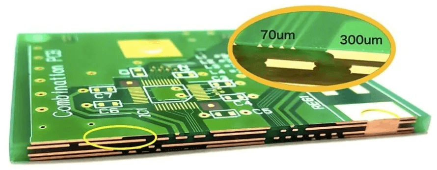
Heavy copper PCBs are specialized printed circuit boards designed with significantly thicker copper layers than conventional PCBs. Their enhanced copper thickness enables higher current-carrying capacity, improved thermal performance, greater mechanical strength, and increased long-term durability.
As electric vehicles, renewable energy systems, battery storage, industrial automation, power converters, motor drives, and high-power electronics continue to expand, demand for Heavy Copper PCB technology is increasing rapidly. Unlike conventional PCB manufacturing, producing heavy copper circuit boards requires specialized etching, plating, lamination, thermal management, and inspection processes.
Selecting the right Heavy Copper PCB Manufacturer is therefore critical for applications where electrical performance, thermal reliability, mechanical durability, and long service life are essential.
This guide introduces 15 leading Heavy Copper PCB Manufacturers selected for their capabilities in heavy copper fabrication, high-current PCB production, multilayer technology, engineering support, and applications across automotive, industrial, energy, aerospace, and power electronics markets.
What Is a Heavy Copper PCB?
A Heavy Copper PCB is generally defined as a printed circuit board manufactured with copper thickness of approximately 3 oz/ft² (105 μm) or greater on one or more layers.
Conventional PCBs commonly use 1 oz/ft² copper, equivalent to approximately 35 μm. Heavy copper designs use substantially thicker copper to support higher current loads and improve heat dissipation.
Typical copper weights include:
| Copper Weight | Approximate Copper Thickness |
|---|---|
| 1 oz | 35 μm |
| 2 oz | 70 μm |
| 3 oz | 105 μm |
| 4 oz | 140 μm |
| 6 oz | 210 μm |
| 10 oz | 350 μm |
| 15 oz | 525 μm |
| 20 oz | 700 μm |
The actual finished copper thickness can vary depending on the manufacturing process, starting foil thickness, and additional electroplating.
Ultra-heavy copper designs can reach 10 oz, 15 oz, 20 oz, or even higher copper weights in selected applications. These boards are particularly valuable in high-power systems where conventional PCB traces cannot provide sufficient current capacity without becoming excessively wide.
The manufacturing process is considerably more demanding than standard PCB fabrication.
Deep copper etching must remove large amounts of copper while maintaining accurate line widths and controlled sidewall geometry. Electroplating must also provide consistent copper deposition through plated through-holes and vias, particularly when thick copper layers create challenging aspect ratios.
For this reason, a qualified Heavy Copper PCB Manufacturer needs specialized process control, equipment, engineering expertise, and inspection capabilities.
Key Advantages of Heavy Copper PCB Technology
Heavy copper circuit boards offer several advantages over conventional PCB constructions. Their most important benefits include higher current capacity, improved thermal management, enhanced mechanical strength, and better resistance to harsh operating conditions.
1. Higher Current-Carrying Capacity
The most obvious advantage of heavy copper is its ability to carry substantially more current.
Increasing copper thickness reduces electrical resistance and allows designers to carry higher currents without requiring extremely wide traces. For example, a 4 oz copper layer can provide significantly greater current capacity than a comparable 1 oz copper layer when the trace geometry and thermal conditions are appropriately designed.
This makes Heavy Copper PCB technology particularly suitable for:
- Power converters
- Battery management systems
- Motor controllers
- Inverters
- EV power electronics
- Industrial power supplies
- Renewable energy equipment
- High-current switching systems
2. Improved Thermal Management
Copper is an excellent thermal conductor. A thicker copper layer can distribute heat laterally across the PCB and help move heat away from high-power components.
When combined with thermal vias, copper-filled vias, copper coins, metal heat spreaders, or other thermal structures, heavy copper construction can become an important part of the overall thermal-management strategy.
This is particularly valuable for systems that operate continuously at high power or in environments with limited cooling space.
3. Greater Mechanical Durability
Thicker copper structures can improve the mechanical robustness of a PCB.
Heavy copper boards can provide improved resistance to mechanical stress, vibration, shock, and localized thermal cycling. This makes them attractive for automotive, aerospace, industrial, and other demanding applications.
4. Reduced Need for Additional Power Hardware
A well-designed heavy copper PCB can integrate current distribution and thermal management directly into the circuit board.
Depending on the application, this can reduce or eliminate the need for separate busbars, current distribution bars, or additional heat-spreading structures.
This approach can simplify system architecture and reduce interconnect complexity.
5. Longer Service Life
Lower conductor resistance and improved thermal distribution can help reduce operating temperatures.
Lower temperatures can decrease thermal stress on copper conductors, solder joints, laminates, and electronic components. As a result, a properly engineered heavy copper PCB can contribute to improved system reliability and service life.
6. Higher Power Density
Heavy copper multilayer boards allow designers to combine high-current power paths with controlled-impedance signal routing within a compact PCB structure.
This is particularly important for modern power electronics, where designers need to reduce system size while simultaneously increasing power density.
Heavy Copper PCB Applications
Because of their electrical, thermal, and mechanical advantages, heavy copper circuit boards are used across a wide range of industries.
Typical applications include:
- Electric vehicle power electronics
- Battery management systems
- DC-DC converters
- AC-DC power supplies
- Solar inverters
- Wind energy systems
- Energy storage systems
- Motor drives
- Industrial automation
- Welding equipment
- Aerospace electronics
- Defense systems
- High-power RF equipment
- Telecommunications power systems
- Medical power electronics
The growing adoption of wide-bandgap semiconductors such as silicon carbide (SiC) and gallium nitride (GaN) is also increasing the importance of advanced thermal and electrical PCB design.
Top 15 Heavy Copper PCB Manufacturers in 2026
The following companies are presented in alphabetical order rather than as an absolute performance ranking. The selection considers heavy copper manufacturing capability, engineering expertise, industry applications, production scale, quality systems, and support for high-current PCB requirements.
| # | Manufacturer | Country/Region | Key Heavy Copper Capabilities |
|---|---|---|---|
| 1 | Advanced Circuits | USA | Heavy copper prototypes, quick-turn production, NPI |
| 2 | AT&S | Austria | Automotive, high-current, energy and advanced multilayer PCBs |
| 3 | Eltek | Norway | Ultra-heavy copper, power electronics, high-current applications |
| 4 | Gold Phoenix PCB | China | Custom heavy copper PCB manufacturing and rapid prototyping |
| 5 | Kinwong Electronic | China | Automotive, energy storage and heavy copper PCB solutions |
| 6 | PCBWay | China | 3–20 oz copper options, prototypes and production |
| 7 | RayMing Technology | China | Cost-effective heavy copper PCB manufacturing and DFM |
| 8 | Sanmina | USA | High-reliability PCB manufacturing and turnkey electronics |
| 9 | SCHWEIZER Electronic | Germany | Automotive power electronics and embedded technologies |
| 10 | Shengyi Technology | China | High-current laminates and advanced PCB materials |
| 11 | Sierra Circuits | USA | High-precision multilayer and heavy copper PCBs |
| 12 | Tripod Technology | Taiwan | High-volume heavy copper PCB production |
| 13 | TTM Technologies | USA | Aerospace, defense, RF and high-power PCB solutions |
| 14 | Kingda | China | Custom heavy copper, multilayer power PCB and industrial applications |
| 15 | Würth Elektronik | Germany | Automotive power electronics, busbars and power modules |
1. Advanced Circuits
Advanced Circuits is a well-known U.S. PCB manufacturer offering prototype and production services for demanding circuit board applications.
Its capabilities are particularly relevant to engineers developing high-current electronic products that require rapid prototyping and reliable PCB fabrication.
Key Capabilities
- Heavy Copper PCB prototyping
- Quick-turn PCB manufacturing
- New product introduction (NPI) support
- High-current PCB applications
- Engineering support
- Domestic U.S. manufacturing capabilities
Advanced Circuits can be a suitable option for engineering teams that prioritize rapid development and prototype-to-production transitions.
2. AT&S
AT&S is an established European PCB manufacturer with extensive experience in advanced PCB technologies.
Its capabilities cover demanding automotive, energy, industrial, and high-performance electronic applications where electrical reliability and thermal management are important.
Key Capabilities
- High-current PCB solutions
- Automotive electronics
- Energy and storage applications
- Advanced multilayer PCB technology
- High-reliability manufacturing
- Advanced engineering and R&D capabilities
AT&S is particularly relevant for customers requiring sophisticated PCB architectures and high levels of process control.
3. Eltek
Eltek is known for PCB solutions designed for demanding power electronics applications.
Its heavy copper capabilities are particularly relevant to applications requiring high current capacity, improved heat dissipation, and long-term reliability.
Key Capabilities
- Ultra-heavy copper processing
- Heavy copper multilayer PCBs
- High-current power electronics
- Industrial applications
- Energy applications
- Advanced thermal-management solutions
For applications requiring exceptionally thick copper layers, the manufacturer’s actual maximum copper weight and layer configuration should always be confirmed during engineering review.
4. Gold Phoenix PCB
Gold Phoenix PCB provides customized PCB manufacturing solutions for industrial control systems, power converters, renewable energy equipment, and high-current electronics.
The company focuses on flexible production, rapid response, engineering support, and quality control for projects ranging from prototypes to production quantities.
Key Capabilities
- Heavy Copper PCB manufacturing
- Rapid-turn PCB production
- Multilayer PCB fabrication
- Renewable energy applications
- Industrial power electronics
- Prototype-to-production support
Its flexible production model can be useful for customers that need customized copper thickness, layer structures, and production volumes.
5. Kinwong Electronic
Kinwong Electronic provides PCB solutions for automotive electronics, energy storage systems, industrial equipment, and power electronics.
Heavy copper technology is particularly valuable in these applications because high-current paths and thermal management are often critical to overall system performance.
Key Capabilities
- Automotive electronics
- Energy storage applications
- Heavy copper PCB technology
- High-current circuit boards
- Industrial power applications
- High-reliability manufacturing
For EV and energy-storage applications, heavy copper technology can help address the electrical and thermal requirements associated with high-power systems.
6. PCBWay
PCBWay is a widely recognized PCB manufacturing service provider offering prototype and production PCB fabrication.
Its heavy copper PCB capabilities cover a range of copper weights, including applications requiring substantially thicker copper than conventional 1 oz designs.
Key Capabilities
- Approximately 3–20 oz copper options for applicable designs
- Heavy copper multilayer PCBs
- Rapid prototyping
- Cost-effective PCB production
- Engineering support
- Global customer service
PCBWay can be attractive to startups, engineers, OEMs, and development teams seeking a combination of prototype flexibility and production scalability.
7. RayMing Technology
RayMing Technology provides customized PCB manufacturing services for industrial, automotive, energy, and power electronics applications.
Its engineering support includes DFM review and assistance with the transition from prototype development to production.
Key Capabilities
- Heavy Copper PCB manufacturing
- DFM engineering support
- Prototype-to-production services
- Multilayer PCB fabrication
- Industrial power applications
- Customized manufacturing
For complex heavy copper designs, engineering collaboration during the pre-production stage can help identify trace-width, copper-weight, via, and thermal-management issues before fabrication begins.
8. Sanmina
Sanmina provides electronics manufacturing services and PCB-related manufacturing capabilities for industrial, medical, aerospace, defense, communications, and other high-reliability markets.
Its major strength is its broader electronics manufacturing ecosystem, which can cover product development, manufacturing, testing, supply chain management, and production.
Key Capabilities
- Turnkey electronics manufacturing
- PCB assembly
- High-reliability electronics
- Industrial power electronics
- Global manufacturing capabilities
- Supply chain management
- Product lifecycle support
Sanmina can be particularly attractive for OEM customers looking for broader electronics manufacturing services rather than PCB fabrication alone.
9. SCHWEIZER Electronic
SCHWEIZER Electronic is a German PCB technology company with a strong focus on automotive and power electronics.
Its technology portfolio includes heavy copper PCB structures and advanced embedded component solutions designed for applications requiring high power density and efficient thermal management.
Key Capabilities
- Automotive power electronics
- Heavy Copper PCB technology
- Embedded component technology
- Advanced thermal management
- High-power applications
- High-reliability PCB solutions
These technologies are relevant to electric mobility, energy management, industrial automation, and other power-intensive systems.
10. Shengyi Technology
Shengyi Technology is primarily recognized for its electronic materials and laminate technologies.
Advanced PCB materials play an important role in heavy copper circuit board performance because dielectric properties, thermal stability, copper adhesion, and mechanical reliability all influence final PCB performance.
Key Capabilities
- Advanced PCB laminates
- High-current PCB material solutions
- Thermal-management materials
- Power electronics materials
- High-performance substrate technologies
- High-reliability material development
When selecting a material supplier for heavy copper PCB projects, designers should evaluate thermal expansion, dielectric performance, copper adhesion, Tg, Td, and compatibility with the intended operating environment.
11. Sierra Circuits
Sierra Circuits specializes in high-performance PCB manufacturing and engineering services for demanding applications.
Its expertise includes multilayer PCBs, high-precision fabrication, aerospace electronics, industrial systems, and power-related applications.
Key Capabilities
- High-precision PCB manufacturing
- Heavy copper multilayer boards
- Aerospace applications
- Engineering support
- Complex PCB fabrication
- Advanced manufacturing processes
For complex high-current designs, manufacturing feedback during the engineering stage can be especially valuable in optimizing copper distribution, thermal structures, and manufacturability.
12. Tripod Technology
Tripod Technology is a major Taiwanese PCB manufacturer serving automotive, industrial, consumer electronics, and other markets.
Its large-scale manufacturing capabilities make it relevant for customers requiring consistent production quality and high-volume PCB manufacturing.
Key Capabilities
- High-volume PCB manufacturing
- Heavy copper multilayer boards
- Automotive applications
- Industrial electronics
- Process consistency
- Advanced manufacturing facilities
For mass production, manufacturers should be evaluated not only on maximum copper thickness but also on process capability, yield, dimensional stability, and long-term production consistency.
13. TTM Technologies
TTM Technologies is a major global PCB manufacturer serving aerospace, defense, telecommunications, automotive, industrial, and high-performance electronics markets.
Its broad technology portfolio includes advanced multilayer PCB solutions and technologies for demanding high-power and RF applications.
Key Capabilities
- Aerospace and defense expertise
- High-power RF PCB solutions
- Advanced multilayer PCB manufacturing
- High-reliability production
- Engineering support
- Global manufacturing capabilities
TTM can be particularly relevant to customers requiring advanced PCB technologies and high-reliability manufacturing for mission-critical applications.
14. Kingda
Kingda specializes in customized PCB manufacturing and provides solutions for industrial power electronics, energy systems, automation equipment, and other applications requiring reliable heavy copper construction.
Its Heavy Copper PCB capabilities can support customers from prototype development through production while emphasizing engineering support, manufacturability, and quality control.
Key Capabilities
- Heavy Copper PCB manufacturing
- Multilayer power PCB technology
- High-current circuit board solutions
- Prototype and production support
- Industrial and energy applications
- Customized PCB manufacturing
- DFM engineering support
For customers developing high-current electronic products, Kingda can provide engineering assistance during the early design stage to evaluate copper weight, layer stackup, trace geometry, thermal management, and manufacturability.
15. Würth Elektronik
Würth Elektronik is a German electronics technology company with extensive expertise in PCB and electronic component technologies.
Its solutions are relevant to automotive, power electronics, industrial automation, and other applications requiring reliable current distribution and thermal management.
Key Capabilities
- Automotive power electronics
- Heavy copper PCB technology
- Busbar solutions
- Power modules
- Industrial automation
- Engineering and technology support
The combination of PCB technology and power-distribution solutions makes this type of supplier relevant to high-current applications where PCB architecture must integrate closely with the overall power system.
Key Capabilities to Evaluate in a Heavy Copper PCB Manufacturer
Choosing a Heavy Copper PCB Manufacturer requires a more detailed evaluation than selecting a conventional PCB supplier.
Important factors include maximum copper weight, multilayer construction capability, copper etching control, plated-through-hole reliability, thermal-management expertise, impedance control, surface finishing, inspection, and assembly capability.
| Capability | What to Evaluate |
|---|---|
| Copper Thickness Range | Verify the actual in-house copper weight capability, from 3 oz to 20 oz or beyond where applicable. |
| Multilayer Stackup | Confirm whether the manufacturer can combine heavy power layers with standard signal layers. |
| Heavy Copper Etching | Evaluate line-width control, etch compensation, sidewall geometry, and copper distribution. |
| Plated Through-Holes | Verify copper plating uniformity and reliability in high-aspect-ratio holes. |
| Thermal Management | Check support for thermal vias, copper coins, heat spreaders, and embedded thermal structures. |
| Impedance Control | Confirm whether controlled-impedance signal layers can be manufactured alongside heavy copper power layers. |
| Surface Finish | Evaluate HASL, ENIG, ENEPIG, hard gold, and other finishes according to assembly requirements. |
| IPC Inspection | Review visual inspection, cross-section analysis, copper thickness measurement, and plating inspection. |
| PCB Assembly | Confirm that the assembly line can handle the high thermal mass of heavy copper boards. |
| Reliability Testing | Review thermal cycling, solderability, via reliability, peel strength, and other applicable tests. |
Why Cross-Section Analysis Matters for Heavy Copper PCBs
Cross-section analysis is one of the most important quality-control methods for heavy copper circuit boards.
A reputable manufacturer should be capable of examining representative PCB samples to verify:
- Copper thickness
- Plated-through-hole thickness
- Via wall quality
- Layer alignment
- Lamination integrity
- Copper-to-laminate adhesion
- Internal defects
- Resin distribution
- Potential voids or delamination
Because heavy copper boards contain substantially more copper than conventional PCBs, their thermal expansion behavior and lamination requirements can be more challenging.
Cross-sectional inspection allows engineers to identify potential manufacturing problems before the product enters mass production.
Customers should therefore request representative cross-section data and relevant quality records when evaluating a new supplier.
Heavy Copper PCB Stackup and Signal Integrity
Multilayer Heavy Copper PCB designs can be considerably more complicated than conventional multilayer boards.
A typical power-oriented stackup may combine heavy copper power layers with thinner signal layers. This creates differences in copper thickness, dielectric spacing, thermal expansion, and impedance behavior.
Controlled-impedance signal layers must still meet their electrical requirements even when adjacent layers contain substantially thicker copper.
For high-speed designs, engineers should evaluate:
- Trace width
- Trace spacing
- Dielectric thickness
- Copper thickness
- Reference-plane configuration
- Differential-pair geometry
- Return-current paths
- Via transitions
- Crosstalk
- Insertion loss
- Thermal effects
A supplier with internal signal-integrity simulation and stackup engineering capabilities can provide significant value during the design stage.
How to Choose the Best Heavy Copper PCB Manufacturer
Choosing the right supplier should not be based solely on the lowest quotation.
A better approach is to evaluate whether the manufacturer can consistently meet your electrical, mechanical, thermal, reliability, and production requirements.
Step 1: Define Copper Weight and Layer Requirements
Specify the exact copper weight required for every layer.
Your engineering package should clearly define:
- Copper weight
- Number of layers
- Layer sequence
- Heavy copper layers
- Standard copper layers
- Finished copper thickness
- Minimum trace width
- Minimum spacing
- Via dimensions
- Board thickness
Clear specifications reduce manufacturing uncertainty and prevent unnecessary engineering changes.
Step 2: Verify In-House Manufacturing Capability
Ask whether the manufacturer actually produces heavy copper PCBs internally.
Do not evaluate a supplier only by its advertised maximum copper thickness.
Confirm:
- Maximum copper weight
- Maximum board dimensions
- Maximum layer count
- Minimum trace and spacing
- Maximum aspect ratio
- Plating capability
- Etching capability
- Production location
- Whether critical processes are outsourced
In-house manufacturing can provide better control over production scheduling, quality, engineering communication, and traceability.
Step 3: Check Relevant Certifications
The required certifications depend on the target industry.
Common quality standards include:
- ISO 9001 for general quality management
- IATF 16949 for automotive applications
- AS9100 for aerospace and defense
- ISO 13485 for medical-device manufacturing
- UL recognition for applicable PCB products
Certification alone does not guarantee product quality, but it provides an important baseline for evaluating a manufacturing partner.
Step 4: Request Cross-Section and Reliability Data
Ask prospective suppliers for representative test data covering:
- Copper thickness
- Plated-hole thickness
- Peel strength
- Thermal cycling
- Solderability
- Via reliability
- Lamination integrity
Actual process data provides a much better indication of manufacturing capability than marketing claims.
Step 5: Evaluate DFM Engineering Expertise
Submit a representative PCB design and review the supplier’s DFM feedback.
A technically strong supplier should be able to identify potential issues involving:
- Copper thickness transitions
- Trace width
- Etching compensation
- Thermal relief
- Via design
- Copper balancing
- Lamination
- Board warpage
- Heat dissipation
- Assembly constraints
Useful engineering feedback before production can prevent expensive redesigns later.
Step 6: Evaluate Heavy Copper PCB Assembly Capability
If you require both PCB fabrication and assembly, confirm that the manufacturer understands the thermal characteristics of heavy copper boards.
Heavy copper increases the thermal mass of the PCB.
During reflow soldering, insufficient thermal energy can result in inconsistent solder joint formation, particularly around large copper planes and heavy copper pads.
The assembly process should therefore be evaluated for:
- Reflow temperature profiling
- Thermal uniformity
- Solder paste selection
- Pad design
- Component compatibility
- Selective soldering
- Wave soldering
- Inspection and testing
Step 7: Consider Logistics and Total Cost
Lead time, shipping distance, customs requirements, engineering communication, and supply-chain stability can significantly influence the real cost of a PCB project.
A supplier with a slightly higher unit price may still offer lower total cost if it provides:
- Better yield
- Fewer engineering revisions
- Shorter lead times
- Lower defect rates
- More reliable delivery
- Better technical support
- Stronger traceability
For heavy copper projects, total cost of ownership is often more important than the initial PCB quotation.
Heavy Copper PCB Manufacturing Challenges
Manufacturing heavy copper circuit boards introduces several challenges that do not exist, or are less significant, in standard PCB production.
Copper Etching
The thicker the copper, the more difficult it becomes to achieve accurate etching.
Insufficient etching can cause unwanted copper bridges and shorts, while excessive etching can reduce trace width and create dimensional deviations.
Copper Plating
Thick copper structures require carefully controlled plating processes.
Uniform copper deposition is particularly important inside plated-through-holes and vias because inadequate plating can reduce electrical and mechanical reliability.
Lamination
Heavy copper features can create significant differences in local thickness.
The manufacturer must carefully manage resin flow, pressure, temperature, copper distribution, and material selection during lamination.
Board Warpage
Uneven copper distribution can contribute to PCB warpage.
Balanced stackup design and appropriate copper distribution are therefore essential for large multilayer heavy copper boards.
Thermal Expansion
Copper and laminate materials have different coefficients of thermal expansion.
Repeated thermal cycling can place stress on plated holes, solder joints, and interfaces.
Material selection and stackup engineering are consequently critical for long-life applications.
Heavy Copper PCB vs. Standard PCB
| Feature | Standard PCB | Heavy Copper PCB |
|---|---|---|
| Typical Copper Weight | 1–2 oz | 3 oz and above |
| Current Capacity | Moderate | High to very high |
| Thermal Performance | Standard | Improved |
| Mechanical Strength | Standard | Higher |
| Etching Difficulty | Lower | Higher |
| Plating Requirements | Standard | More demanding |
| Manufacturing Cost | Lower | Higher |
| Manufacturing Complexity | Moderate | High |
| Typical Applications | Consumer and general electronics | Power electronics, EVs, energy, industrial systems |
| Power Density Potential | Moderate | High |
Heavy copper PCBs are not necessarily the best choice for every electronic product. For low-power applications, standard PCB construction may provide a more economical solution.
The primary value of heavy copper technology appears when high current, heat dissipation, mechanical durability, or power density becomes a critical design requirement.
Heavy Copper PCB Materials and Design Considerations
Material selection is another important part of heavy copper PCB development.
Depending on the application, engineers may need to consider:
- FR-4 laminates
- High-Tg materials
- Halogen-free materials
- High thermal-performance laminates
- Metal-backed structures
- Ceramic or specialized substrate technologies
Important material parameters include:
Tg, Td, coefficient of thermal expansion (CTE), dielectric constant, dissipation factor, thermal conductivity, copper adhesion, and mechanical strength.
For automotive and industrial products that operate over wide temperature ranges, high-Tg and low-CTE materials may provide additional reliability advantages.
Heavy Copper PCBs for Electric Vehicles and Renewable Energy
Electric vehicles are one of the major application areas driving demand for high-current PCB technologies.
EV systems contain high-power electronics such as:
- Battery management systems
- On-board chargers
- DC-DC converters
- Inverters
- Motor controllers
- Power distribution systems
These systems require efficient current distribution and thermal management in compact spaces.
Renewable energy systems have similar requirements.
Solar inverters, energy storage systems, wind power converters, and grid-connected power electronics must handle substantial electrical loads while maintaining long-term reliability.
As power density continues to increase, heavy copper PCB technology provides an effective way to integrate electrical and thermal functions into a compact PCB structure.
The Role of SiC and GaN in Heavy Copper PCB Design
Wide-bandgap semiconductor technologies such as silicon carbide (SiC) and gallium nitride (GaN) are enabling power electronics to operate at higher switching frequencies, voltages, and temperatures.
These technologies can improve power-conversion efficiency and reduce system size, but they also create new challenges for PCB designers.
Higher switching speeds can increase:
- Electromagnetic interference
- Voltage overshoot
- Switching losses
- Thermal concentration
- Current density
- Layout sensitivity
Consequently, heavy copper PCB design increasingly needs to consider electrical and thermal performance simultaneously.
Copper thickness alone is not sufficient.
Engineers must also optimize current paths, return paths, loop areas, thermal vias, component placement, grounding, impedance, and power-plane geometry.
Why Early Supplier Evaluation Is Important
The best time to evaluate a Heavy Copper PCB Manufacturer is before the final PCB layout is completed.
An experienced supplier can provide DFM feedback during the design stage and help engineers determine:
- Appropriate copper weight
- Trace width
- Copper spacing
- Layer stackup
- Thermal structures
- Via dimensions
- Copper balancing
- Lamination requirements
- Manufacturing tolerances
Early engineering collaboration can prevent multiple prototype iterations and reduce the risk of manufacturing-related redesigns.
For complex power electronics, the PCB manufacturer should ideally be treated as an engineering partner rather than simply a supplier.
Conclusion
Choosing the right Heavy Copper PCB Manufacturer can have a major impact on the electrical performance, thermal management, reliability, production yield, and total cost of a high-power electronic product.
The 15 manufacturers discussed in this guide represent a range of capabilities across prototype development, high-volume production, automotive electronics, industrial power systems, renewable energy, aerospace, defense, and advanced power electronics.
When evaluating suppliers, do not focus solely on maximum copper thickness or unit price. Instead, assess the complete manufacturing capability, including copper etching, electroplating, multilayer lamination, thermal management, impedance control, inspection, reliability testing, DFM engineering, and PCB assembly.
The continued adoption of EVs, energy storage, renewable power systems, SiC and GaN semiconductors, and high-density industrial electronics will further increase the importance of advanced Heavy Copper PCB Manufacturing.
Working with a capable supplier from the design stage can help optimize copper distribution, stackup architecture, thermal performance, current capacity, and manufacturability before the first prototype is built.
For customized high-current and power-electronics applications, Kingda can provide Heavy Copper PCB manufacturing and engineering support from prototype development to production, helping customers develop reliable circuit boards for demanding electrical and thermal environments.