Top 15 Six-Layer PCB Manufacturers in 2026: A Complete Guide to Choosing the Right Supplier
A reliable six-layer PCB manufacturer combines signal integrity, thermal management, manufacturing precision, and compact circuit design to produce boards capable of meeting the demanding requirements of modern electronic products. Choosing the right manufacturing partner can directly affect product performance, development costs, reliability, and time to market.
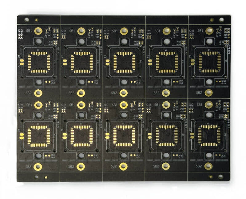
As electronic systems become smaller, faster, and more functionally complex, engineers increasingly rely on multilayer PCB manufacturing to accommodate dense routing, high-speed interfaces, power distribution, and electromagnetic compatibility requirements. Compared with conventional four-layer boards, six-layer PCBs provide additional routing resources and greater flexibility for separating power, ground, and signal networks.
Six-layer boards are widely used in telecommunications, medical electronics, automotive systems, industrial automation, networking equipment, aerospace electronics, and other applications where electrical performance and reliability are critical.
This guide introduces 15 notable six-layer PCB manufacturers to consider in 2026. It also explains the technical capabilities, manufacturing processes, quality certifications, and supplier-selection criteria that should be evaluated before starting a new PCB project.
Note: The ranking below is an editorial comparison based on manufacturing capabilities, application experience, technology coverage, quality systems, engineering support, and market presence. It should not be interpreted as an official industry ranking.
What Is a Six-Layer PCB?
A six-layer PCB is a multilayer printed circuit board containing six conductive copper layers separated by dielectric insulating materials. The copper layers are interconnected using plated through-holes, blind vias, buried vias, or microvias, depending on the board’s design and manufacturing requirements.
A typical six-layer PCB stackup may include:
- Top signal layer
- Internal signal or power layer
- Ground layer
- Power layer
- Internal signal layer
- Bottom signal layer
However, there is no single universal six-layer stackup. The optimal configuration depends on signal speed, impedance requirements, power distribution, thermal conditions, component density, EMC requirements, and manufacturing constraints.
For high-speed applications, engineers often place signal layers adjacent to continuous reference planes to control impedance and reduce electromagnetic coupling. Ground planes can also provide low-inductance return paths, which are essential for maintaining signal integrity.
Compared with a four-layer PCB, a six-layer board provides additional routing channels without necessarily increasing the board’s physical footprint. This makes six-layer technology particularly attractive for compact electronic products with high component density.
Common Applications of Six-Layer PCBs
Six-layer PCBs are commonly used in:
- Telecommunications and networking equipment
- 5G infrastructure
- Medical imaging systems
- Industrial automation controllers
- Automotive ECUs
- Advanced consumer electronics
- Data communication equipment
- Aerospace and avionics systems
- Power management equipment
- Embedded computing systems
The combination of routing density, controlled impedance, power distribution, and compact construction makes six-layer PCBs a practical solution for many medium-to-high-complexity electronic products.
Advantages of Six-Layer PCB Technology
Compared with simpler multilayer structures, a well-designed six-layer PCB can provide improved routing flexibility, signal integrity, electromagnetic compatibility, and power distribution.
1. Improved Signal Integrity
A properly designed six-layer stackup can place high-speed signal traces close to continuous ground or power reference planes. This reduces loop area, improves return-current paths, and helps control impedance.
For high-speed digital interfaces, RF circuits, and other sensitive signals, controlled stackup design is essential for minimizing reflections, crosstalk, and transmission-line losses.
2. Higher Routing Density
Additional copper layers provide engineers with more routing space. This makes six-layer boards suitable for complex circuits that cannot be routed efficiently on two- or four-layer PCBs.
More routing layers can also help designers avoid excessive trace congestion and reduce the need for unnecessarily large board dimensions.
3. Better Power Distribution
Dedicated power and ground layers can create lower-impedance power distribution networks. Proper plane design can reduce voltage fluctuations and improve power integrity, particularly in systems containing high-speed processors, communication modules, and other power-sensitive devices.
4. Controlled Impedance
Professional six-layer PCB manufacturers can optimize dielectric thickness, copper thickness, trace width, and layer spacing to achieve the required controlled impedance.
Common impedance targets may include 50 Ω for RF and single-ended high-speed signals and 90 Ω or 100 Ω differential impedance for certain high-speed interfaces, although the correct target always depends on the interface specification.
5. Reduced EMI and Crosstalk
Ground planes positioned between signal layers can help reduce electromagnetic coupling. Carefully controlled layer spacing and routing geometry can further reduce crosstalk between adjacent circuits.
This is particularly important in telecommunications, automotive electronics, industrial controls, and medical equipment.
6. More Compact Product Design
Additional routing capacity allows designers to integrate more functions into a smaller PCB footprint. This is valuable for products where enclosure size and weight are important design constraints.
7. Improved Thermal Management
Copper planes can contribute to heat spreading, although PCB thermal performance depends on more than the number of copper layers. Copper weight, thermal vias, component placement, dielectric materials, board thickness, and external cooling methods all influence the final thermal performance.
Therefore, a professional manufacturer should evaluate thermal requirements during the PCB design and DFM process rather than simply adding copper layers.
Top 15 Six-Layer PCB Manufacturers to Consider in 2026
The following companies represent a range of PCB manufacturing capabilities, from rapid prototyping and cost-effective production to advanced multilayer, high-reliability, HDI, automotive, aerospace, and medical PCB manufacturing.
| Rank | Manufacturer | Region | Key Strengths | Typical Focus |
|---|---|---|---|---|
| 1 | PCBWay | China | Multilayer, HDI, rapid prototyping | Prototype to production |
| 2 | JLCPCB | China | Cost-effective manufacturing, fast turnaround | Prototypes and volume production |
| 3 | TTM Technologies | USA | High-reliability and advanced PCB technologies | Aerospace, defense, medical |
| 4 | Sanmina | USA | Complex PCB and turnkey manufacturing | Medical, aerospace, industrial |
| 5 | Tripod Technology | Taiwan | High-volume multilayer manufacturing | Consumer and communications |
| 6 | Kingboard Holdings | Hong Kong | PCB and laminate manufacturing | Commercial and industrial electronics |
| 7 | Eltek | Norway | Heavy copper and specialized PCBs | High-reliability applications |
| 8 | Viasion Technology | China | Custom multilayer PCB manufacturing | Prototype to mass production |
| 9 | Shengyi Electronics | China | High-frequency and high-speed materials | Communications and automotive |
| 10 | AT&S | Austria | Advanced interconnect and IC substrate technologies | Automotive, medical, semiconductor |
| 11 | Advanced Circuits | USA | Rapid PCB prototyping and production | Engineering and OEM projects |
| 12 | Würth Elektronik | Germany | Engineering-oriented PCB solutions | Industrial and automotive |
| 13 | Gold Phoenix PCB | China | Custom multilayer PCB manufacturing | Industrial and electronic products |
| 14 | RayMing Technology | China | Rapid prototyping and multilayer PCB production | Prototype and production |
| 15 | Sierra Circuits | USA | High-reliability PCB manufacturing | Aerospace, defense, medical |
The appropriate supplier depends heavily on the requirements of the individual project. A manufacturer optimized for low-cost prototypes may not be the best choice for aerospace or medical production. Likewise, a high-end manufacturer may not be the most economical option for a simple consumer-electronics project.
1. PCBWay
PCBWay is a well-known PCB manufacturing service provider offering a broad range of manufacturing capabilities, including conventional multilayer PCBs, HDI boards, rigid-flex PCBs, and PCB prototypes.
Its manufacturing model is suitable for engineers, startups, OEMs, and electronics developers looking for a supplier capable of supporting projects from initial prototypes through larger production runs.
Key Capabilities
- Six-layer PCB manufacturing
- Multilayer and HDI PCB production
- Rapid PCB prototyping
- Rigid and rigid-flex PCB options
- PCB assembly services
- Global customer support
- Engineering and manufacturing services
For development teams that need flexibility across different PCB technologies, a broad manufacturing portfolio can simplify supplier management.
2. JLCPCB
JLCPCB is widely recognized for cost-effective PCB manufacturing and rapid turnaround services. Its automated production environment makes it particularly attractive to engineers and product developers who require economical prototypes or production quantities.
Key Capabilities
- Cost-effective six-layer PCB production
- Rapid manufacturing turnaround
- Automated manufacturing processes
- Prototype and production support
- PCB assembly services
- International shipping
For budget-sensitive development projects, JLCPCB can be considered when the technical requirements fit its manufacturing capabilities.
3. TTM Technologies
TTM Technologies is a major PCB manufacturer serving demanding industries such as aerospace, defense, medical, automotive, and telecommunications.
Its capabilities are particularly relevant to applications where PCB reliability, advanced interconnect technology, material performance, and process control are critical.
Key Capabilities
- High-reliability multilayer PCBs
- Aerospace and defense experience
- Advanced HDI technologies
- High-speed and RF PCB capabilities
- Engineering support
- High-reliability manufacturing
TTM Technologies can be a strong candidate for projects where reliability and technical performance are more important than minimizing unit cost.
4. Sanmina
Sanmina provides broad electronics manufacturing services, including PCB manufacturing, PCB assembly, system integration, and other production services.
Its capabilities are relevant to complex electronic systems used in industries such as medical technology, aerospace, defense, industrial equipment, and communications.
Key Capabilities
- Complex multilayer PCB manufacturing
- Turnkey electronics manufacturing
- PCB assembly and system integration
- Medical and aerospace experience
- Global manufacturing infrastructure
- Engineering support
A supplier capable of supporting both PCB production and downstream assembly can reduce supply-chain complexity for OEM customers.
5. Tripod Technology
Tripod Technology is a Taiwan-based PCB manufacturer known for large-scale production of multilayer printed circuit boards.
Its products serve markets including consumer electronics, communications, automotive electronics, and networking applications.
Key Capabilities
- High-volume PCB manufacturing
- Advanced multilayer production
- Consumer electronics expertise
- Automotive PCB applications
- Communications and networking support
- Large-scale supply-chain capabilities
Tripod is particularly relevant to customers that require high-volume production and consistent manufacturing output.
6. Kingboard Holdings
Kingboard Holdings has extensive experience in PCB and laminate manufacturing. Its broad industrial presence enables it to support various commercial, industrial, and telecommunications applications.
Key Capabilities
- Large-scale manufacturing
- PCB and laminate production
- Multilayer PCB capabilities
- Commercial electronics support
- Industrial applications
- Global market presence
Material and laminate expertise can be an important consideration when PCB performance depends heavily on dielectric characteristics and thermal stability.
7. Eltek
Eltek specializes in high-reliability PCB technologies, including heavy-copper and specialized PCB solutions.
Heavy-copper technology is particularly useful for applications that require high current-carrying capability, improved thermal conduction, or enhanced mechanical robustness.
Key Capabilities
- Heavy-copper PCB technology
- High-reliability manufacturing
- Specialized materials
- Advanced PCB construction
- Industrial and demanding applications
- Strict quality control
For high-current or harsh-environment applications, engineers should evaluate copper thickness, thermal requirements, current density, and plating quality in addition to the basic layer count.
8. Viasion Technology
Viasion Technology provides custom PCB manufacturing and PCB assembly services ranging from prototypes to production quantities.
Its capabilities cover rigid, flexible, and rigid-flex PCBs, making it suitable for customers requiring different PCB technologies within a single supply chain.
Key Capabilities
- Six-layer and multilayer PCB manufacturing
- PCB assembly
- SMT and THT assembly
- Rigid and flexible PCBs
- Rigid-flex PCB manufacturing
- Prototype-to-production support
- Engineering and quality control
When evaluating a custom six-layer PCB supplier, customers should consider not only fabrication capabilities but also whether the supplier can provide DFM feedback, engineering communication, and production support.
9. Shengyi Electronics
Shengyi Electronics is associated with advanced laminate and materials technologies used in high-frequency and high-speed electronic applications.
Material selection becomes increasingly important as signal frequencies rise because dielectric constant, dissipation factor, thermal stability, and dimensional stability can affect signal performance.
Key Capabilities
- High-frequency PCB materials
- High-speed applications
- Advanced laminate technologies
- Telecommunications applications
- Automotive electronics
- Signal-integrity-oriented materials
For high-speed six-layer PCB designs, choosing the appropriate laminate can be just as important as optimizing the copper routing.
10. AT&S
AT&S is a major European PCB manufacturer known for advanced interconnect technologies, IC substrates, and high-end PCB solutions.
Its technologies support demanding industries including automotive electronics, medical systems, industrial applications, aerospace, and semiconductor-related products.
Key Capabilities
- Advanced interconnect technologies
- High-density PCB manufacturing
- IC substrate technologies
- Automotive electronics
- Medical electronics
- High-end multilayer solutions
For technically demanding products, advanced interconnect capability can provide additional design freedom while maintaining compact form factors.
11. Advanced Circuits
Advanced Circuits provides PCB manufacturing services for engineers, startups, OEMs, and electronics manufacturers.
Its product portfolio includes prototype PCB manufacturing and production services, making it useful for companies that need to transition from development to manufacturing.
Key Capabilities
- Rapid PCB prototyping
- Six-layer PCB production
- Prototype-to-production services
- Engineering support
- Online quotation and manufacturing services
- Production PCB manufacturing
Fast prototype turnaround can be especially valuable during iterative hardware development, where engineers may need multiple PCB revisions before design verification is complete.
12. Würth Elektronik
Würth Elektronik provides PCB technologies and engineering-oriented electronics solutions for industrial, automotive, medical, and communication applications.
Its engineering capabilities make it relevant to customers who need technical support during PCB development rather than simply purchasing finished boards.
Key Capabilities
- Multilayer PCB solutions
- Industrial PCB applications
- Automotive electronics
- Engineering support
- Custom manufacturing
- Quality-focused production
A supplier with strong engineering support can help identify stackup, impedance, component-clearance, and manufacturability problems before they become expensive production issues.
13. Gold Phoenix PCB
Gold Phoenix PCB provides custom PCB manufacturing services for multilayer and other PCB configurations.
Its capabilities can support applications including telecommunications, automotive electronics, industrial equipment, and consumer electronics.
Key Capabilities
- Custom six-layer PCB manufacturing
- Multilayer PCB production
- Prototype services
- Volume manufacturing
- Telecommunications applications
- Industrial electronics
When selecting a supplier for custom six-layer boards, customers should confirm minimum trace width and spacing, via capabilities, copper thickness, surface finishes, and available materials before placing an order.
14. RayMing Technology
RayMing Technology provides PCB prototyping and manufacturing services for customers across different industries.
Its product range includes multilayer, HDI, rigid-flex, and other specialized PCB technologies.
Key Capabilities
- Rapid PCB prototyping
- Multilayer PCB manufacturing
- HDI PCB capabilities
- Rigid-flex PCB solutions
- Various surface finishes
- Prototype and production services
Rapid prototyping can shorten development cycles, particularly when hardware teams need to validate electrical performance, mechanical integration, and firmware functionality simultaneously.
15. Sierra Circuits
Sierra Circuits is known for high-reliability PCB manufacturing and engineering services, with a strong focus on technically demanding applications.
Its capabilities are relevant to aerospace, defense, medical, automotive, and other applications where PCB performance and reliability are critical.
Key Capabilities
- High-reliability PCB manufacturing
- High-precision PCB fabrication
- Aerospace and defense applications
- Advanced engineering support
- Multilayer PCB manufacturing
- Quality and testing services
For mission-critical electronics, supplier evaluation should focus on process control, traceability, testing capability, material management, and long-term reliability rather than simply comparing PCB prices.
Key Capabilities to Look for in a Leading Six-Layer PCB Manufacturer
Not every manufacturer offering six-layer PCB production provides the same level of engineering or quality control. A reliable supplier should be able to demonstrate technical competence throughout the PCB fabrication process.
| Capability | What to Look For |
|---|---|
| Stackup design | Controlled impedance, symmetrical construction, optimized reference planes |
| Materials | FR-4, high-Tg materials, Rogers, Isola, polyimide, and other application-specific laminates |
| Trace and spacing | Capability appropriate for the required density and production yield |
| Via technology | Through vias, blind vias, buried vias, and microvias where required |
| Copper thickness | Standard and heavy-copper options based on current and thermal requirements |
| Surface finish | HASL, lead-free HASL, ENIG, OSP, immersion tin, hard gold, etc. |
| Testing | AOI, electrical testing, flying probe, ICT, X-ray inspection where applicable |
| Engineering | DFM, stackup review, impedance analysis, manufacturability feedback |
| Production | Prototype, low-volume, and mass-production capabilities |
| Quality systems | Appropriate ISO, automotive, medical, aerospace, or other industry certifications |
Stackup Design
A six-layer PCB stackup should be designed according to the electrical requirements of the project rather than simply assigning one function to each copper layer.
Important considerations include:
- Signal-to-plane spacing
- Dielectric thickness
- Copper thickness
- Controlled impedance
- Differential-pair routing
- Return-current paths
- Power distribution
- Crosstalk
- EMC performance
A professional PCB manufacturer should be able to review the proposed stackup and recommend adjustments before production.
Material Selection
Standard FR-4 may be sufficient for many six-layer PCBs. However, higher-speed or higher-temperature applications may require specialized materials.
Material selection should consider:
- Dielectric constant
- Dissipation factor
- Glass transition temperature
- Decomposition temperature
- Thermal expansion
- Moisture resistance
- Dimensional stability
- Frequency-dependent electrical characteristics
Selecting a material only according to price can create signal-integrity or reliability problems later in the product lifecycle.
Via Technology
The required via structure depends on component density and routing complexity.
Common options include:
- Through-hole vias
- Blind vias
- Buried vias
- Microvias
- Via-in-pad structures
Not every six-layer board requires HDI technology. However, high-density designs may benefit from microvias and sequential lamination when conventional through-hole routing becomes restrictive.
Surface Finish
Surface finish influences solderability, corrosion resistance, contact reliability, cost, and shelf life.
Common finishes include:
- HASL
- Lead-free HASL
- ENIG
- OSP
- Immersion tin
- Immersion silver
- Hard gold
The correct finish should be selected according to the assembly process and end-use requirements.
Testing and Inspection
Reliable manufacturers should maintain an appropriate inspection and testing strategy.
Typical inspection methods include:
- Automated Optical Inspection (AOI)
- Electrical testing
- Flying probe testing
- X-ray inspection
- Dimensional inspection
- Microsection analysis
- Solderability testing
- Impedance testing
The exact test combination should be determined by the PCB’s complexity and application risk.
Why DFM Is Critical for Six-Layer PCB Manufacturing
Design for Manufacturability (DFM) is one of the most important services a PCB supplier can provide before fabrication begins.
A DFM review can identify problems involving:
- Minimum trace width
- Trace-to-pad spacing
- Hole diameter
- Annular ring
- Copper-to-edge clearance
- Solder-mask openings
- Via structures
- Layer registration
- Component clearances
- Impedance requirements
- Manufacturing tolerances
Identifying these issues before production is considerably less expensive than correcting them after boards have been fabricated.
A capable six-layer PCB manufacturer should therefore provide engineering feedback rather than simply accepting Gerber files and starting production.
Six-Layer PCB Manufacturing Process
The manufacturing process typically involves multiple controlled stages.
1. Engineering Review
The manufacturer reviews Gerber files, drill files, stackup information, material requirements, copper thickness, impedance specifications, and production tolerances.
2. Material Preparation
The appropriate copper-clad laminates and prepreg materials are selected according to the approved stackup.
3. Inner-Layer Fabrication
The inner copper layers are cleaned, coated with photoresist, exposed, developed, and etched to form the required circuitry.
4. Optical Inspection
AOI systems inspect the inner layers for open circuits, shorts, pattern defects, and dimensional abnormalities.
5. Lamination
The individual circuit layers are aligned and laminated under controlled temperature and pressure.
Layer alignment is particularly important because registration errors can affect vias, pads, and fine-pitch components.
6. Drilling
Mechanical drilling and, where necessary, laser drilling create the required through-holes and microvias.
7. Copper Plating
The drilled holes are metallized and plated to create reliable electrical connections between PCB layers.
8. Outer-Layer Fabrication
The outer copper layers are patterned and etched according to the final circuit design.
9. Solder Mask and Silkscreen
Solder mask is applied to protect exposed copper and reduce the risk of solder bridging. Silkscreen is then applied for component references, markings, and other identification information.
10. Surface Finishing
The appropriate surface finish is applied according to the assembly and application requirements.
11. Electrical Testing
The completed PCB is tested for electrical continuity and isolation to identify open and short circuits.
12. Final Inspection and Packaging
The finished boards undergo final quality inspection before packaging and shipment.
How to Choose the Best Six-Layer PCB Manufacturer
Selecting the right supplier requires more than comparing quotations. A six-layer PCB can contain complex electrical and manufacturing requirements, so supplier selection should consider technical capability, quality, communication, lead time, and total cost.
1. Define Your Technical Requirements First
Before requesting quotations, prepare the essential PCB specifications, including:
- Board dimensions
- Layer count
- Board thickness
- Copper thickness
- Minimum trace and spacing
- Via structure
- Surface finish
- Material requirements
- Controlled impedance requirements
- Quantity
- Expected production volume
A clear technical specification allows manufacturers to provide more accurate quotations and manufacturing recommendations.
2. Verify Quality Certifications
Certification requirements should match the target industry.
For example:
- ISO 9001 – General quality management
- ISO 14001 – Environmental management
- IATF 16949 – Automotive quality management
- ISO 13485 – Medical-device quality management
- AS9100 – Aerospace quality management
Certification alone does not guarantee PCB quality, but it provides evidence that the supplier operates within a structured quality-management system.
3. Request a DFM Review
A supplier that performs a meaningful DFM review can identify manufacturing risks before production.
Ask whether the manufacturer can review:
- Stackup
- Trace and spacing
- Drill sizes
- Via structures
- Copper distribution
- Impedance requirements
- Solder-mask design
- Board-edge clearances
4. Evaluate Prototype and Production Lead Times
Prototype development often requires rapid turnaround because engineers may need multiple design iterations.
For production projects, consistency and capacity are generally more important than simply achieving the shortest possible lead time.
Always confirm whether the quoted lead time includes engineering review, fabrication, testing, and shipping.
5. Evaluate Engineering Communication
Technical communication is often overlooked during supplier selection.
A reliable manufacturing partner should respond clearly to questions involving:
- Stackup
- Material selection
- Manufacturing tolerances
- Impedance
- DFM issues
- Quality problems
- Production changes
Poor communication during quotation and engineering review can create much larger problems after production begins.
6. Review Testing Coverage
Ask the manufacturer which tests are included in the quotation.
Depending on the application, these may include:
- AOI
- Electrical testing
- Flying probe
- X-ray inspection
- Microsection analysis
- Impedance testing
- Dimensional inspection
For high-reliability applications, test records and traceability can be especially important.
7. Consider the Total Cost of Ownership
The lowest PCB unit price does not necessarily represent the lowest project cost.
A supplier with a slightly higher quotation may provide better value if it offers:
- Higher production yield
- Better DFM support
- Lower defect rates
- More reliable delivery
- Better engineering communication
- Stronger testing capabilities
- More consistent quality
The real objective should be to minimize the total cost of manufacturing and product development.
Six-Layer PCB Manufacturer Comparison: What Matters Most?
Different projects require different supplier priorities.
For Low-Cost Prototypes
Prioritize:
- Competitive pricing
- Fast quotations
- Rapid prototype turnaround
- Easy online ordering
- Flexible minimum order quantities
For High-Volume Consumer Electronics
Prioritize:
- Production capacity
- Automation
- Yield
- Supply-chain stability
- Consistent quality
- Cost control
For Automotive Electronics
Prioritize:
- IATF 16949-related quality systems
- Automotive-grade materials
- Traceability
- Thermal reliability
- Long-term production consistency
For Medical Electronics
Prioritize:
- ISO 13485-related quality systems
- Traceability
- Process control
- Electrical testing
- High reliability
- Documentation
For Aerospace and Defense
Prioritize:
- AS9100-related quality systems
- High-reliability materials
- Advanced inspection
- Traceability
- Engineering expertise
- Tight process control
Why Kingda Can Be a Valuable Six-Layer PCB Manufacturing Partner
For companies seeking a flexible and engineering-focused six-layer PCB manufacturer, Kingda can be positioned as a manufacturing partner capable of supporting projects from PCB fabrication through production requirements.
A strong supplier relationship should go beyond simply manufacturing boards. It should include engineering communication, DFM support, material selection, stackup optimization, quality control, testing, and production coordination.
Kingda Six-Layer PCB Capabilities
Key capabilities to consider include:
- Six-layer PCB manufacturing
- Multilayer PCB fabrication
- Controlled-impedance PCB manufacturing
- High-density PCB solutions
- Prototype and production manufacturing
- PCB assembly support
- DFM engineering review
- Surface-finish options
- Electrical testing and inspection
- Customized PCB manufacturing
For projects involving high-speed signals, compact layouts, or demanding operating conditions, the manufacturing partner should be involved early in the design process.
Early collaboration makes it easier to optimize the stackup, material selection, trace geometry, via structures, and manufacturing tolerances before the design reaches production.
Frequently Asked Questions About Six-Layer PCBs
Is a Six-Layer PCB Better Than a Four-Layer PCB?
Not necessarily. A six-layer PCB is better when the design requires additional routing capacity, controlled impedance, improved power distribution, greater component density, or better EMC performance.
For a simple circuit, a four-layer PCB may be more economical and easier to manufacture.
How Much Does a Six-Layer PCB Cost?
The cost depends on factors such as:
- Board dimensions
- Quantity
- Material
- Copper thickness
- Board thickness
- Minimum trace and spacing
- Via technology
- Surface finish
- Testing requirements
- Production location
Therefore, there is no universal price for a six-layer PCB.
Does a Six-Layer PCB Require HDI?
No. A six-layer PCB can be manufactured using conventional through-hole vias. HDI technology becomes useful when routing density, component pitch, or board size makes conventional vias insufficient.
What Materials Can Be Used for Six-Layer PCBs?
Standard FR-4 is widely used, while high-Tg FR-4, low-loss materials, PTFE-based laminates, Rogers materials, Isola materials, and polyimide may be selected for specialized applications.
How Long Does Six-Layer PCB Manufacturing Take?
Lead time varies according to board complexity, quantity, materials, testing requirements, and factory capacity. Prototype and mass-production lead times should therefore be confirmed with the manufacturer based on the actual Gerber files and specifications.
Final Thoughts
The demand for six-layer PCBs continues to grow as electronic products become smaller, faster, and more complex. Telecommunications infrastructure, automotive electronics, industrial automation, medical equipment, networking systems, and high-performance computing all require PCB technologies capable of supporting increasingly sophisticated electrical designs.
However, choosing a six-layer PCB supplier should not be based solely on price.
The right manufacturing partner should provide an appropriate combination of PCB manufacturing capability, engineering expertise, material options, quality management, testing, production capacity, communication, and delivery performance.
Some manufacturers are particularly competitive for rapid prototyping and cost-sensitive projects. Others focus on high-volume production, while specialized suppliers may be better suited to aerospace, automotive, medical, high-frequency, or high-reliability applications.
Before selecting a supplier, evaluate the manufacturer’s stackup capabilities, minimum trace and spacing, via technology, material portfolio, surface finishes, testing procedures, certifications, DFM support, and production capacity.
For companies developing a new six-layer PCB, working with the manufacturer early in the design cycle can significantly reduce manufacturing risks. A professional supplier can help identify potential problems before fabrication and optimize the design for yield, reliability, cost, and performance.
Kingda can support customers looking for reliable six-layer and multilayer PCB manufacturing solutions, from prototype development and DFM review to production and quality inspection. By combining engineering support with controlled manufacturing processes, Kingda aims to help customers shorten development cycles, improve PCB reliability, and achieve more predictable production results.
If you are preparing a new six-layer PCB project, providing the Gerber files, stackup requirements, BOM, technical specifications, expected quantity, and target application will allow the manufacturing team to evaluate the project more accurately and recommend an appropriate production solution.