PCB Component Layout and Routing Design Guide for High Performance Circuit Boards
A successful electronic product begins with a well-designed circuit board. In modern electronics development, PCB design plays a critical role in determining electrical performance, signal integrity, thermal management, and manufacturing reliability.
The process of arranging components and designing signal paths on a printed circuit board requires careful consideration of electrical characteristics, production requirements, and long-term product stability.
A professional PCB design approach helps reduce signal interference, improve circuit performance, and ensure smooth transition from prototype development to mass production.
Component placement is one of the most important stages in the PCB development process. A reasonable layout can shorten signal paths, reduce electromagnetic interference, and improve overall circuit efficiency.
During PCB layout, engineers need to consider:
- Signal flow direction
- Power distribution
- Heat generation
- Component accessibility
- Manufacturing requirements
- Electromagnetic compatibility (EMC)
Poor component arrangement may cause signal degradation, difficult assembly, and increased production costs.
Professional PCB assembly service providers usually review PCB layouts before production to identify potential manufacturing and reliability issues.
Learn more about GoPCB manufacturing capabilities:
When designing multilayer circuit boards, signal traces on adjacent layers should avoid running in the same direction.
Using vertical routing between different layers helps reduce electromagnetic coupling and unnecessary interference.
Recommended practices include:
- Keep adjacent layer traces perpendicular when possible
- Use ground planes for signal isolation
- Separate sensitive signals from high-speed signals
This approach improves signal integrity and reduces crosstalk problems.
During PCB routing, unused floating traces should be avoided because they may create antenna effects.
Open-ended copper traces can:
- Receive external interference
- Increase electromagnetic radiation
- Affect high-frequency signal performance
Engineers should ensure that all unused connections are properly terminated or removed.
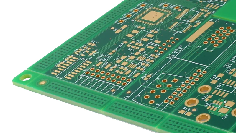
For high-performance electronic products, professional PCB manufacturing partners can provide design optimization support before fabrication.
Explore GoPCB PCB production solutions:
Shorter trace lengths generally provide better electrical performance.
Long signal paths may introduce:
- Signal delay
- Noise problems
- Reflection issues
- Increased electromagnetic interference
For circuits containing high-speed signals, memory interfaces, RF modules, or communication systems, controlling trace length is essential.
Engineers should carefully plan component placement before beginning detailed routing.
High-speed PCB designs require accurate impedance control.
When trace width changes suddenly, the characteristic impedance may become inconsistent, causing signal reflection.
Important impedance design considerations include:
- Stable trace width
- Proper dielectric thickness
- Correct copper thickness
- Controlled layer stack-up
Professional PCB suppliers can help customers select suitable materials and stack-up structures for impedance-controlled designs.
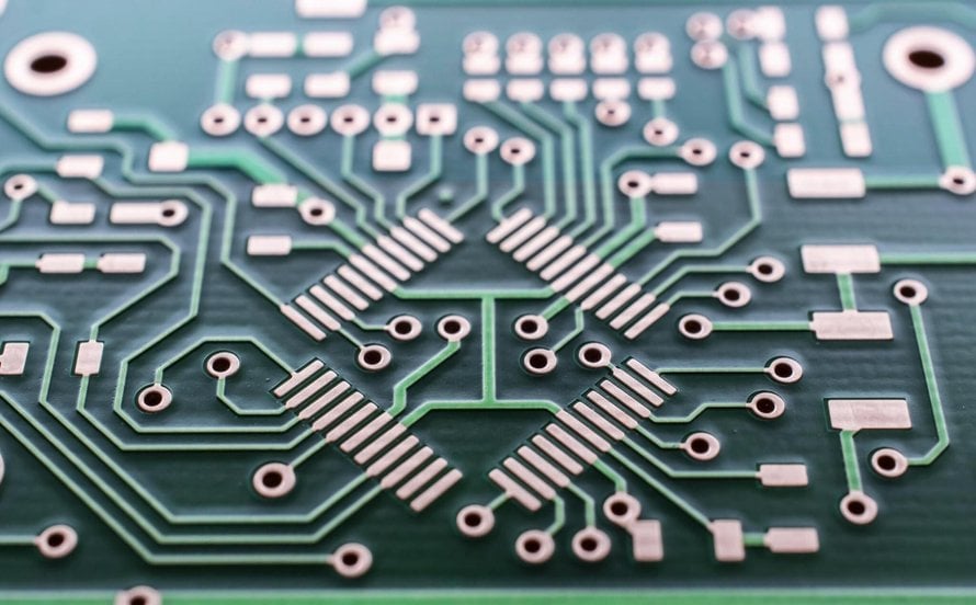
Sharp corners in PCB traces can create unnecessary signal reflection and electromagnetic radiation.
Traditional PCB design recommendations suggest avoiding 90-degree routing corners.
Better solutions include:
- Using two 45-degree bends
- Applying curved routing methods
- Maintaining smooth signal transitions
These improvements are especially important for high-frequency and high-speed circuits.
Decoupling capacitors help stabilize power supply signals and reduce high-frequency noise.
They should be placed:
- Close to power pins
- Near integrated circuits
- With short connection paths
Proper capacitor placement improves circuit stability and reduces power fluctuations.
The 3W rule is commonly used in high-speed PCB layout design.
It means the spacing between two signal traces should generally be at least three times the width of the trace.
Benefits include:
- Reduced signal crosstalk
- Improved electromagnetic compatibility
- Better signal integrity
For sensitive applications such as communication equipment and industrial electronics, following spacing rules can significantly improve performance.
Ground loops can increase electromagnetic radiation and introduce unwanted noise.
A good grounding strategy focuses on minimizing loop area between:
- Signal traces
- Return paths
- Ground planes
A smaller current loop helps reduce external interference and improves system reliability.
Modern multilayer PCB structures often use dedicated ground planes to provide stable return paths.
For high-frequency or sensitive signals, shielding methods may be required.
Common shielding approaches include:
- Ground guard traces
- Copper shielding areas
- Ground planes around critical signals
- Proper grounding connections
Effective shielding reduces external interference and improves signal transmission quality.
GoPCB provides professional PCB prototype and manufacturing solutions for advanced electronic applications.
High-speed circuit designs must consider transmission line effects.
If trace length becomes related to signal wavelength, resonance problems may occur.
Engineers should analyze:
- Signal frequency
- Trace length
- Transmission speed
- Material properties
Proper simulation and design verification help prevent unexpected signal integrity issues.
A complete PCB development process requires close cooperation between design engineers and manufacturers.
Professional PCB design support can help optimize:
- Component placement
- Routing structure
- Layer configuration
- Manufacturing compatibility
- Assembly efficiency
Early design verification reduces production risks and improves product reliability.
Before sending files for manufacturing, engineers should check:

Confirm:
- Correct schematic connections
- Complete routing
- Proper spacing rules
- Accurate component footprints
Review:
- Minimum trace width
- Via size
- Solder mask requirements
- Assembly limitations
Consider:
- Electrical testing points
- Functional testing methods
- Inspection requirements
These steps ensure smooth transition from design to production.
Effective PCB design requires careful planning of component placement, routing strategies, impedance control, and signal protection.
Following professional PCB layout principles helps improve electrical performance, reduce interference, and increase manufacturing success.
Whether developing prototypes or preparing large-scale production, choosing an experienced partner with strong engineering capability is essential.
GoPCB provides complete solutions including PCB manufacturing, PCB assembly service, prototype development, and customized circuit board production for customers worldwide.