10 Common PCB Design Mistakes and How to Avoid Them
A successful electronic product begins with a reliable circuit board design. During the development process, even small layout mistakes can cause manufacturing difficulties, electrical failures, signal problems, and increased production costs.
Professional Printed Circuit Board Design requires careful consideration of electrical performance, mechanical requirements, manufacturing capability, and assembly standards.
Understanding common design problems before production helps engineers improve product reliability and shorten development cycles. This article introduces the most common PCB Design Mistakes and explains how to avoid them during the design stage.
1. Incorrect Layer Definition and Stack-Up Planning
Why Layer Definition Matters in PCB Design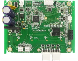
One of the most common mistakes in PCB projects is incorrect layer configuration.
For example, designers may accidentally define the wrong layer as the top or bottom layer, resulting in:
- Incorrect component placement
- Poor soldering performance
- Manufacturing confusion
- Assembly problems
A proper PCB layer stack-up should clearly define:
- Signal layers
- Ground planes
- Power layers
- Copper thickness
- Dielectric materials
Before manufacturing begins, engineers should verify the complete layer structure through professional PCB Design Services to ensure the design matches production requirements.
For advanced multilayer applications, proper planning of Multilayer PCB Solutions helps improve electrical performance and manufacturing reliability.
2. Copper Pour Too Close to the Board Edge
Maintain Proper Copper Clearance
Large copper areas are commonly used for:
- Ground connections
- Heat dissipation
- Current distribution
- Signal shielding
However, placing copper too close to the PCB edge can create manufacturing problems.
During mechanical routing or board cutting, insufficient clearance may cause:
- Copper exposure
- Edge defects
- Reduced insulation distance
- Potential short circuits
Engineers should maintain proper spacing between copper areas and the board outline according to manufacturing guidelines.
A reliable PCB Manufacturing Process requires accurate control of copper distribution and edge clearance.
3. Using Copper Fill Objects Instead of Proper Pads
Avoid Incorrect Pad Design
During PCB layout, some designers use copper-filled shapes to create component pads because they appear similar visually.
However, these objects may not generate correct manufacturing data.
Potential problems include:
- Incorrect solder mask openings
- Difficult component assembly
- Poor solder reliability
- Manufacturing data errors
Standard component pads should always be created using professional PCB design tools with correct pad definitions.
Proper pad structures are an important part of PCB Layout Optimization.
For engineers requiring complete production support, our PCB Manufacturing Services provide reliable fabrication solutions from prototype to mass production.
4. Incorrect Electrical Connections Between Pads and Traces
Prevent Power and Ground Connection Errors
PCB designs often include multiple power networks and ground connections.
A common mistake occurs when designers create incorrect thermal connections or isolated copper areas.
Possible consequences include:
- Open circuits
- Power instability
- Signal interference
- Circuit failures
Designers should carefully check:
- Net connections
- Copper zones
- Thermal relief settings
- Ground plane structures
Using Design Rule Check (DRC) tools before manufacturing can prevent many electrical connection issues.
5. Improper Silkscreen and Reference Mark Design
Optimize PCB Markings for Assembly
Silkscreen information helps manufacturers identify:
- Component locations
- Polarity marks
- Assembly references
- Test points
However, incorrect silkscreen design may cause:
- Overlapping characters
- Hidden component markings
- Difficult inspection
- Assembly errors
Common mistakes include:
- Text placed on solder pads
- Font size too small
- Excessively large labels
- Incorrect reference positions
Optimized silkscreen design improves assembly efficiency and product quality.
6. Incorrect SMD Pad Length Design
Ensure Reliable SMT Assembly
Surface mount technology requires precise pad dimensions.
If SMD pads are too short:
- Testing becomes difficult
- Solder joints may become unstable
- Inspection accuracy decreases
For densely populated circuit boards, pad dimensions must match:
- Component specifications
- Solder paste requirements
- Assembly processes
Professional PCB Assembly Services ensure that component placement and soldering processes meet industry standards.
Learn more about our PCB Assembly Services for high-quality electronic manufacturing solutions.
7. Incorrect Single-Sided Pad Opening Design
Avoid Manufacturing Data Problems
Some PCB designs use single-sided pads without proper drilling information.
If drilling requirements are not clearly defined, manufacturing systems may generate incorrect drill files.
Problems may include:
- Missing holes
- Incorrect hole positions
- Production delays
Engineers should clearly define:
- Pad types
- Hole sizes
- Drill information
- Manufacturing requirements
Complete production documentation is essential for successful PCB fabrication.
8. Overlapping Drill Holes
Prevent PCB Manufacturing Defects
Overlapping holes are another common PCB design problem.
When multiple holes share the same location:
- Drills may break
- PCB layers may become damaged
- Insulation structures may fail
This issue is especially serious in multilayer boards where precise drilling accuracy is required.
Before production, engineers should check:
- Via locations
- Component holes
- Mechanical holes
- Drill file accuracy
Proper verification during the PCB Manufacturing Process helps avoid unnecessary production waste.
9. Excessive Use of Copper Filling Areas
Optimize Copper Pour Design
Copper filling areas are useful for improving:
- Ground stability
- Heat distribution
- Signal shielding
However, excessive copper regions or extremely thin copper connections can create problems.
Potential issues include:
- Increased manufacturing difficulty
- Incomplete exposure during imaging
- Data processing problems
A balanced copper design should consider:
- Manufacturing capability
- Electrical requirements
- Thermal performance
Proper PCB Layout Optimization improves both electrical reliability and production efficiency.
10. Incorrect Use of Graphic Layers
Maintain Clear PCB Documentation
Another frequent PCB design problem is incorrect usage of graphic layers.
Some designers place unnecessary information on manufacturing layers, creating confusion.
Examples include:
- Extra copper layers
- Incorrect mechanical drawings
- Unnecessary graphic objects
A professional PCB design file should contain:
- Clearly defined layers
- Accurate fabrication information
- Proper documentation
Clean design files allow manufacturers to produce boards faster and reduce communication problems.
Additional PCB Design Considerations
Thermal Management and Copper Pour Design
Modern electronic devices generate increasing amounts of heat.
PCB designers should consider:
- Thermal vias
- Copper areas
- Component placement
- Heat dissipation paths
Good thermal design improves product lifetime and reliability.
Signal Integrity and EMI Control
High-speed electronic products require careful control of:
- Signal routing
- Impedance
- Ground planes
- Differential pairs
Poor routing can result in:
- Signal distortion
- Noise problems
- Electromagnetic interference
Professional engineers use simulation and verification tools to improve signal performance.
How Professional PCB Manufacturers Help Avoid Design Problems
A reliable PCB partner provides support throughout the entire development process:
Engineering Review
Before production, engineers review:
- PCB files
- Gerber data
- Layer stack-up
- Manufacturing requirements
Design Verification
Advanced verification includes:
- DRC checking
- Electrical testing
- Manufacturing feasibility analysis
Production Control
During manufacturing, quality control focuses on:
- Line width accuracy
- Copper thickness
- Surface finishing
- Inspection standards
Final Assembly Testing
Complete testing ensures finished boards meet performance requirements.
For more information about professional production capabilities, visit our PCB Assembly Manufacturer solutions.
Conclusion
Avoiding common PCB design errors is essential for creating reliable electronic products.
From layer definition and copper clearance to pad design and manufacturing documentation, every detail affects the final product quality.
By following professional design standards and working with experienced manufacturers, engineers can reduce production risks, improve efficiency, and achieve better product performance.
Choosing reliable PCB Design Services and advanced manufacturing support ensures that every stage from prototype development to mass production meets industry requirements.
Whether developing consumer electronics, industrial equipment, medical devices, or communication products, optimized Printed Circuit Board Design is the foundation of successful electronic innovation.