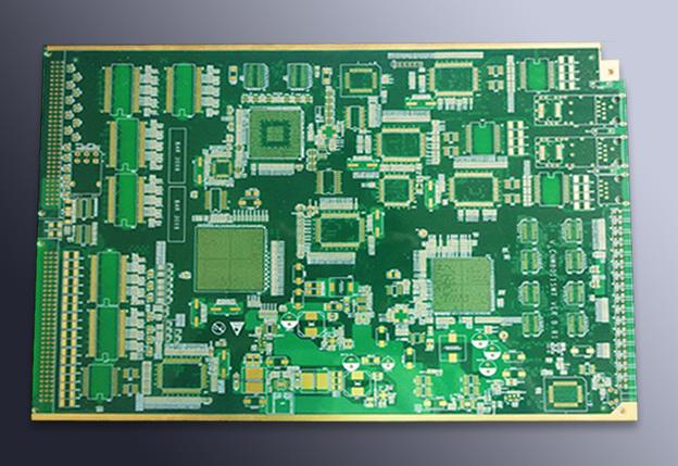
With the continuous development of high-density electronic products, the requirements for miniaturization, high-speed signal transmission, and high-density interconnection have increased significantly. HDI PCBs are widely used in smartphones, communication equipment, automotive electronics, industrial control systems, and other advanced electronic products because they can provide higher wiring density within a limited board area.
As one of the key technologies in HDI manufacturing, CO₂ laser drilling is mainly used to form microvias in dielectric materials. Compared with conventional mechanical drilling, laser drilling provides higher flexibility and is particularly suitable for small-diameter holes and high-density interconnection structures.
Depending on the material structure and manufacturing requirements, CO₂ laser drilling can generally be divided into several process methods, including the direct drilling method, the copper window method, direct drilling on the resin surface, and the ultra-thin copper foil direct ablation method.
1. Direct Drilling Method
The direct drilling process uses the main control system of the laser drilling equipment to adjust the laser beam diameter according to the required hole size. The laser beam is then directly applied to the surface of the dielectric material to form the required hole without first creating a copper window in the surface copper foil.
This method has a relatively simple process flow because it eliminates the need for additional copper-window formation. During operation, however, accurate laser positioning and stable control of the dielectric material are essential. Any deviation in the laser beam position can directly affect the location, diameter, and profile of the resulting microvia.
The direct drilling method is particularly suitable for material structures in which the dielectric resin is directly exposed to the laser beam. The laser energy must be carefully adjusted according to the resin type, dielectric thickness, copper thickness, and required hole diameter. Excessive laser energy may cause excessive resin removal or damage to the surrounding material, while insufficient energy may result in incomplete drilling and residual material at the bottom of the hole.
2. Copper-Window Drilling Method
The copper window method is a conventional process for HDI PCB manufacturing. In this process, a defined opening is first created in the copper foil above the target area. The exposed dielectric resin is then removed using a laser beam to form the required microvia.
The conventional process generally involves exposure, development, and etching to form the copper window. After the copper opening has been prepared, the laser beam is directed through the window to remove the dielectric resin underneath.
2.1 Enlarged Copper Window Process
In the conventional process, the diameter of the copper window may be designed to closely correspond to the diameter of the target hole. However, if the process is not carefully controlled, positional deviation of the copper window may occur. This can result in misalignment between the microvia and the center of the underlying target pad.
Copper-window deviation may be caused by dimensional changes in the PCB material, expansion and contraction of the substrate, or deformation of the film used during image transfer. These factors can become more significant as the PCB becomes thinner and the design density increases.
For this reason, one practical approach is to enlarge the copper window slightly to provide additional process tolerance. For example, when the required microvia diameter is approximately 0.15 mm, the diameter of the underlying pad may be approximately 0.25 mm, while the copper window may be designed to approximately 0.30 mm, depending on the actual design rules and manufacturing capabilities.
The larger copper window provides greater tolerance during CO₂ laser drilling. It can reduce the risk that the laser spot will fail to align with the copper opening and can help prevent incomplete half-holes, residual copper, or partially drilled areas from appearing on the board surface.
However, the copper-window diameter cannot be increased indefinitely. An excessively large window occupies additional routing space and may reduce the available area for adjacent circuitry. Therefore, the appropriate window size should be determined according to the microvia diameter, pad size, PCB layer structure, design density, and manufacturing tolerance.
2.2 Copper-Window Laser Drilling Process
Another form of the copper-window process uses RCC (Resin Coated Copper) as the material structure. An RCC layer is laminated onto the PCB surface, and the required copper pattern is subsequently formed using photochemical processing.
After the copper window has been created, the laser beam is directed toward the target position to remove the exposed dielectric resin and form the microvia. The laser beam is controlled by galvanometer scanning mirrors and focused onto the target area through an F-theta lens system.
The scanning system enables the laser beam to move rapidly between programmed coordinates, allowing microvias to be drilled individually and accurately according to the PCB design data.
For a microvia with a diameter of approximately 0.15 mm, multiple laser pulses may be applied to the same location. The first pulse provides sufficient energy to remove the majority of the dielectric resin, while subsequent pulses can be used to remove residual material from the hole wall and bottom.
The purpose of these additional pulses is not simply to enlarge the hole but also to improve the cleanliness and dimensional consistency of the microvia. Excessive laser exposure, however, may cause excessive resin recession, rough hole walls, or damage to the surrounding dielectric material.
Cross-sectional SEM analysis can be used to evaluate the resulting microvias. Properly controlled laser energy can provide good control over the hole diameter, hole profile, and cleanliness of the hole bottom.
When the target pad is relatively small, the available process margin becomes limited. This is particularly challenging for offset microvias, stacked microvias, and other high-density structures. In such applications, accurate registration between the laser-drilled hole, copper window, and underlying target pad becomes increasingly important.
3. Direct Drilling on the Resin Surface
In the process of directly forming holes on the resin surface, the CO₂ laser drilling process is applied directly to exposed dielectric resin. Several different material structures can be used for this type of process.
A. Resin-Coated Copper Structure
A resin-coated copper material can be laminated onto the upper layer of the inner-layer board. The copper foil in the target area is then removed by etching, exposing the resin surface.
The CO₂ laser can subsequently form the required holes directly in the exposed resin. After laser drilling, the holes undergo the appropriate plating processes to establish reliable electrical interconnection with the underlying copper structure.
B. FR-4 Prepreg and Copper Foil Structure
The dielectric structure can also be formed using FR-4 prepreg combined with copper foil instead of RCC material. This configuration provides another option for HDI PCB manufacturing.
The selection between FR-4 prepreg and other dielectric materials depends on the required board thickness, dielectric properties, thermal performance, laser absorption characteristics, and compatibility with the subsequent manufacturing processes.
C. Photosensitive Resin-Coated Copper Foil
Photosensitive resin-coated copper foil can also be used as the dielectric structure. The photosensitive resin can be selectively processed to create the required pattern before or during the subsequent laser drilling process.
This type of material structure may provide greater flexibility for high-density PCB applications where fine features and controlled dielectric thickness are required.
D. Dry-Film Dielectric Layer
A dry film can be used as the dielectric layer, followed by lamination of copper foil. This approach can provide a relatively thin dielectric structure and may be suitable for applications requiring fine-pitch interconnections and small microvias.
The thickness uniformity of the dry film is particularly important because variations in dielectric thickness can affect laser absorption and consequently influence the final microvia diameter and depth.
E. Other Thermosetting Film and Copper Foil Structures
Other types of thermosetting dielectric films can also be combined with copper foil to create suitable PCB structures. The material selection should take into account electrical performance, thermal resistance, dielectric thickness, laser absorption characteristics, mechanical properties, and compatibility with subsequent plating and lamination processes.
4. Ultra-Thin Copper Foil Direct Ablation Process
Another important method is the ultra-thin copper foil direct ablation process. In this process, resin-coated copper foil is laminated onto the core board. After lamination, the copper foil thickness can be reduced to approximately 5 μm through a controlled semi-etching process.
The ultra-thin copper surface can then undergo a black-oxide or similar surface treatment to improve its ability to absorb laser energy. When the energy of the CO₂ laser beam is appropriately controlled, the laser can directly ablate the ultra-thin copper foil and the underlying resin to form the required microvia.
The basic principle is that the treated copper surface has improved absorption of the laser energy. By controlling the laser power, pulse width, beam diameter, and number of pulses, the copper layer and dielectric resin can be removed in a controlled manner.
One of the most difficult aspects of this process is maintaining a uniform copper thickness after the semi-etching process. Any significant variation in copper thickness can change the amount of laser energy absorbed by the copper surface. This can consequently affect the hole diameter, hole profile, and cleanliness of the hole bottom.
Therefore, strict quality and technical requirements should be imposed on the material supplier. The thickness and uniformity of both the copper foil and dielectric layer must be carefully controlled.
For this type of PCB manufacturing process, ultra-thin copper foil with a thickness of approximately 5 μm may be used. The actual material specification should be selected according to the PCB structure and the capabilities of the laser drilling equipment.
5. Key Process Control Requirements
For ultra-thin copper foil and direct laser ablation processes, several factors require particular attention.
First, the material supplier must maintain strict control over the thickness uniformity of the dielectric layer. The dielectric thickness should remain within the specified tolerance range. Uniform dielectric thickness is essential because, under the same laser energy conditions, variations in dielectric thickness can directly affect the accuracy of the hole shape and the cleanliness of the hole bottom.
Second, the laser drilling parameters must be optimized according to the actual material structure. Important parameters include laser power, pulse width, pulse frequency, beam diameter, focal position, and the number of laser pulses.
These parameters should be optimized as a complete process rather than adjusted independently. A stable combination of laser parameters can help achieve consistent hole diameter, hole depth, sidewall quality, and bottom cleanliness.
Third, the subsequent desmear process must be carefully controlled. After laser drilling, resin residues and carbonized material may remain on the hole wall or at the bottom of the microvia. If these residues are not effectively removed, they may adversely affect subsequent electroless copper deposition and electroplating.
An optimized desmear process can ensure that the bottom of the microvia is clean and free of residual resin and contaminants. This is particularly important for achieving reliable electrical connections between the microvia and the underlying copper pad.
In addition, the hole wall should be inspected after laser drilling and desmear. Excessive resin recession, carbonized residue, rough hole walls, or insufficient cleaning can all affect the quality of subsequent electroless copper plating and electroplating.
Conclusion
In the manufacturing of HDI PCBs, CO₂ laser drilling is an important technology for forming microvias and achieving high-density interconnections. Different process methods, including direct drilling, the copper window method, direct resin-surface drilling, and the ultra-thin copper foil direct ablation method, have different characteristics and applicable material structures.
The selection of the appropriate process should be based on the PCB layer structure, dielectric thickness, copper foil thickness, microvia diameter, pad size, registration accuracy, production volume, and equipment capabilities.
At the same time, stable material quality, accurate laser parameter control, precise registration, effective, and reliable subsequent plating processes are essential for achieving high-quality microvias.
By optimizing these factors throughout the manufacturing process, Kingda can improve HDI PCBs production consistency, reduce manufacturing defects, and achieve reliable electrical and mechanical performance for high-density electronic products.