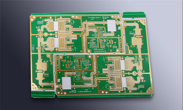
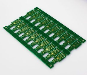
The rapid development of the industrial sector has brought both opportunities and challenges to the electronics industry. A PCB blank board becomes a finished PCBA after undergoing the complete SMT placement and soldering process at a professional PCBA manufacturing facility.
Today, electronic products are becoming increasingly compact, lightweight, multifunctional, and highly integrated. As a result, modern electronic products place higher demands on PCB manufacturing and assembly technologies. To achieve miniaturization, high component density, and reliable electrical performance, SMT assembly technology has become an essential manufacturing process.
Surface Mount Technology (SMT) enables electronic components to be mounted directly onto the surface of a PCB. Compared with traditional through-hole assembly, SMT can significantly reduce component size, improve assembly density, shorten electrical connection paths, and increase production efficiency. It is therefore widely used in consumer electronics, communications equipment, industrial control systems, automotive electronics, medical equipment, and other electronic products.
Kingda is committed to providing professional PCB prototyping and SMT assembly services. With advanced production equipment, extensive manufacturing experience, and standardized production processes, Kingda can handle high-precision SMT assembly, complex component placement, special assembly requirements, and rapid SMT prototyping.
By combining automated equipment with strict process control and comprehensive quality inspection, Kingda can meet demanding industrial requirements while improving production efficiency and delivery speed. The main stages of the SMT assembly process are described below.
1. Programming and Placement Setup
The first step in the SMT assembly process is to prepare the placement program according to the customer’s BOM, component placement drawing, PCB design files, and other relevant manufacturing data.
The placement coordinates of each component are programmed into the pick-and-place machine. The machine uses these coordinates to determine the exact position, orientation, and sequence of each component during the automated placement process.
Before mass production, Kingda can perform a first-article assembly according to the customer’s supplied data. The first assembled PCB is then carefully inspected to verify component type, position, orientation, polarity, and other critical parameters.
This first-article verification process helps identify programming errors or data inconsistencies before mass production begins. It can significantly reduce the risk of batch defects and improve overall production efficiency.
2. Solder Paste Printing
Solder paste printing is one of the most important processes in the SMT production line.
During this process, a stainless-steel stencil is accurately aligned with the PCB. Solder paste is then printed through the stencil openings onto the PCB pads where the SMD components will be mounted.
The purpose of the solder paste is to provide the solder material required to form reliable electrical and mechanical connections between the components and PCB pads during reflow soldering.
Before the widespread adoption of printed circuit boards, electronic components were commonly interconnected using direct wiring methods. As electronic products became increasingly complex, conventional wiring could no longer satisfy the requirements for compactness, reliability, and mass production. PCB technology subsequently became a fundamental part of modern electronics manufacturing.
The equipment used for solder paste printing is an automatic stencil printer, which is normally located at the front end of the SMT production line.
Kingda uses high-precision automatic printing equipment and carefully controlled solder paste materials to improve printing consistency and production efficiency. Important parameters such as stencil alignment, printing pressure, squeegee speed, separation speed, and solder paste condition must be properly controlled.
A stable printing process is particularly important for fine-pitch and high-density PCB assemblies. Excessive solder paste may cause solder bridges, while insufficient solder paste may result in weak or incomplete solder joints.
Therefore, accurate stencil design and precise printing control are essential for achieving reliable PCB assembly quality.
3. Component Placement
The next step is to accurately mount SMD components onto their designated positions on the PCB.
The pick-and-place machine automatically picks components from feeders and places them onto the solder paste deposited on the PCB pads. The placement system uses programmed coordinates and optical recognition technology to ensure accurate component positioning.
Modern high-speed placement machines can handle a wide range of component sizes, including very small 0201 components. High placement accuracy is especially important for high-density PCB designs where the distance between adjacent components may be extremely small.
Kingda uses high-speed automatic placement equipment to achieve accurate and stable component placement. The equipment integrates automatic component recognition, precision positioning, programmable placement, and production monitoring functions.
During this process, several factors must be carefully controlled, including component orientation, polarity, placement coordinates, feeder accuracy, and PCB positioning.
Incorrect component placement can lead to electrical failures, soldering defects, or difficulties during subsequent inspection. Therefore, the placement process is a critical stage of the overall SMT assembly process.
4. Reflow Soldering
The primary purpose of reflow soldering is to melt the solder paste at a controlled temperature and then cool it gradually so that the SMD components are securely connected to the PCB.
The equipment used for this process is a multi-zone reflow oven, which is generally located downstream of the pick-and-place machine on the SMT production line.
During the reflow process, the PCB passes through several temperature zones. These normally include preheating, thermal soaking, reflow, and cooling zones.
During preheating, the temperature of the PCB gradually increases to reduce thermal shock. During the soaking stage, the board temperature becomes more uniform and the flux begins to activate. The PCB then enters the reflow zone, where the solder paste reaches its melting temperature and forms solder joints between the SMD components and PCB pads.
Finally, the board enters the cooling zone, where the solder joints solidify and achieve their required mechanical and electrical characteristics.
Kingda uses multi-zone reflow equipment with precise temperature control to provide uniform heating and cooling. This is particularly important for PCBs with high component density, different component sizes, and complex thermal characteristics.
The reflow temperature profile must be optimized according to the solder paste type, PCB thickness, component specifications, and overall assembly structure.
If the temperature is too high or the heating time is too long, sensitive components may be damaged. If the temperature is too low, the solder paste may not melt properly, resulting in insufficient wetting or weak solder joints.
Therefore, precise temperature-profile control is essential for achieving reliable reflow soldering results.
5. Cleaning
The cleaning process is used to remove flux residues and other potentially harmful contaminants remaining on the assembled PCB after soldering.
Depending on the solder paste and flux materials used, cleaning may be performed using dedicated PCB cleaning equipment. The cleaning equipment can be integrated into the production line or operated as an independent offline process.
Effective cleaning is particularly important for electronic products that require high reliability. Residual flux, ionic contamination, dust, and other contaminants may affect electrical insulation and, under certain environmental conditions, may contribute to corrosion or leakage currents.
Therefore, the cleaning method should be selected according to the soldering materials, PCB structure, component types, and final product requirements.
After cleaning, the PCB should be thoroughly dried and inspected to ensure that no excessive moisture or cleaning residue remains.
6. Testing and Inspection
After the soldering process, comprehensive testing and inspection are performed on the finished PCBA.
The inspection process generally covers different assembly configurations, including surface-mounted components, through-hole components, single-sided or double-sided assembly, fine-pitch components, and high-density component arrangements.
Key inspection items include:
- Component quantity and type
- Component placement and orientation
- Solder joint quality
- Missing or incorrectly placed components
- Solder bridges and insufficient solder
- Electrical characteristics
- PCB surface condition
- Overall product appearance
Kingda uses various high-precision inspection technologies, including AOI inspection systems, X-ray inspection equipment, LCR bridge testers, and high-magnification digital microscopes.
AOI inspection can automatically detect many visible assembly defects, including missing components, incorrect component orientation, placement deviation, solder bridges, insufficient solder, and other soldering-related problems.
For hidden solder joints that cannot be fully inspected using conventional optical methods, X-ray inspection can provide additional analysis. This is particularly useful for BGA, QFN, and other components with hidden solder joints.
LCR testing equipment can be used to measure electrical parameters such as resistance, capacitance, and inductance. High-magnification digital microscopes can provide detailed visual inspection of solder joints, component leads, pads, and other small structures.
By combining automated optical inspection, electrical testing, visual inspection, and X-ray analysis where necessary, Kingda can establish a comprehensive quality-control system for PCBA production.
7. Packaging
After passing all required inspections and tests, qualified PCBA products are individually protected and packaged.
Common packaging materials include anti-static bags, ESD-safe foam, anti-static cotton, and plastic trays.
There are two common packaging methods.
The first method is to individually package the PCBA using anti-static bags or ESD-safe protective materials. This is one of the most widely used packaging methods because it helps protect electronic assemblies from electrostatic discharge, dust, moisture, and minor mechanical impact.
The second method is to place the PCBA in dedicated plastic trays. This method is particularly suitable for assemblies with fragile components, protruding pins, sensitive connectors, or other structures that require additional mechanical protection.
The appropriate packaging method should be selected according to the PCB structure, component sensitivity, transportation conditions, storage requirements, and customer specifications.
Proper packaging is an important part of the overall PCB assembly process. Even after a PCBA has passed all manufacturing and inspection procedures, improper handling or packaging may cause component damage, bent pins, solder joint stress, or electrostatic damage.
Therefore, Kingda pays close attention to packaging materials and methods to ensure that finished products remain protected during storage, transportation, and final installation.
Conclusion
The complete SMT assembly process involves multiple interconnected stages, including programming and placement setup, solder paste printing, component placement, reflow soldering, cleaning, testing, inspection, and packaging.
Each stage has a direct impact on the quality, reliability, and service life of the finished electronic product.
Accurate component placement, consistent solder paste printing, precise reflow temperature control, effective cleaning, comprehensive AOI inspection, and appropriate anti-static packaging are all essential for achieving stable and reliable PCBA quality.
With advanced equipment, standardized manufacturing procedures, experienced engineers, and comprehensive quality-control systems, Kingda can provide reliable PCB assembly and SMT manufacturing solutions for a wide range of electronic applications.
By continuously optimizing production processes and inspection standards, Kingda can help customers improve manufacturing efficiency, reduce defects, shorten production cycles, and achieve consistent product quality for high-density and highly integrated electronic products.