How to Prevent PCB Short Circuits During PCB Design
In PCB design and manufacturing, a PCB Short Circuit is one of the most common and costly defects engineers and manufacturers need to prevent. A short circuit can result from incorrect copper routing, overlapping vias, insufficient clearance, improper copper pours, or missing isolation between PCB layers.
The good news is that many short-circuit risks can be identified before fabrication. By combining proper PCB Design Rules, DRC verification, DFM analysis, careful routing practices, and manufacturer-specific design guidelines, engineers can significantly reduce the risk of electrical shorts and production failures.
1. Common Causes of PCB Short Circuits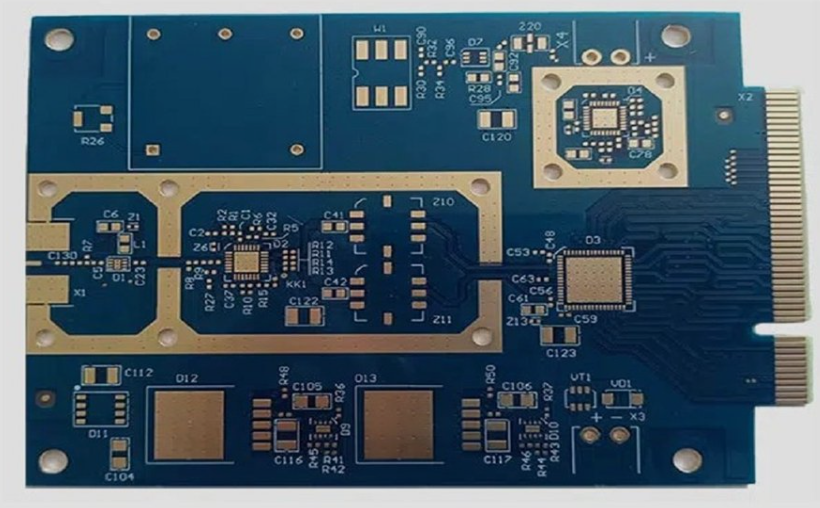
Short circuits introduced during PCB layout are usually caused by unintended connections between different electrical networks. The following examples illustrate several common problems.
Different Networks Connected by Copper Pour
One common problem occurs when copper areas belonging to different networks overlap.
For example, one through-hole may be connected to a negative power network while another hole is connected to a positive power network. If copper is manually added without proper network assignment, the two copper regions may overlap and create an unintended electrical connection.
The underlying causes can include:
- No differentiated clearance rules between positive and negative power networks
- Incorrect manual copper pouring
- Copper assigned to the wrong net
- Incorrect use of solid fills instead of intelligent polygon pours
Most modern PCB design software can identify these problems through Design Rule Check (DRC). However, certain design or configuration errors may prevent the problem from being detected.
For example, a solid fill may cover objects without considering their electrical network properties. Incorrect DRC settings, insufficient clearance values, or the use of non-electrical drawing objects can also allow a potential short circuit to pass the design check.
This is why a professional PCB DFM Analysis should be considered an additional layer of verification before manufacturing.
Overlapping Vias From Different Networks
Another common source of a PCB Short Circuit is overlapping vias connected to different electrical networks.
For example, one via may connect to GND while another connects to VCC. If their drill holes or plated walls overlap because the required spacing has not been maintained, the two networks can become electrically connected.
The problem is particularly important in high-density multilayer PCB designs, where vias are placed very close together.
Designers should therefore define appropriate via-to-via clearance rules according to the PCB manufacturer’s manufacturing capabilities.
Missing Isolation Between PCB Layers
Multilayer PCBs require careful consideration of copper structures on internal layers.
A via may connect an outer layer to another signal or power layer while passing through several internal layers. If the internal layers do not contain the required clearance or anti-pad structure, the via barrel can unintentionally contact copper belonging to another network.
This type of defect can be difficult to identify through visual inspection alone, particularly in high-layer-count boards.
For complex multilayer designs, manufacturers should review the stack-up, via structures, copper clearances, and layer-to-layer relationships before production. GOPCBA provides advanced PCB Manufacturing capabilities for multilayer, HDI, blind/buried-via, and other complex PCB structures.
Insufficient Clearance
Insufficient spacing between traces, pads, vias, copper pours, and other conductive features is another major cause of short circuits.
If the physical clearance between two different networks is below the manufacturing or design requirement, even a small dimensional variation during etching, plating, or registration can create an electrical connection.
The clearance requirements should therefore be defined before routing begins and should account for the actual fabrication capability of the selected manufacturer.
2. How to Prevent PCB Short Circuits During Design
Preventing short circuits should not depend only on a final inspection. A more reliable approach is to establish manufacturing rules and verification procedures from the beginning of the PCB design process.
Establish Manufacturing Rules Before Layout
Before routing a PCB, designers should understand the manufacturer’s manufacturing capabilities, including:
- Minimum trace width
- Minimum trace spacing
- Minimum annular ring
- Minimum mechanical drill size
- Minimum laser drill size
- Via-to-via clearance
- Copper thickness
- Layer registration tolerance
- Solder mask clearance
- PCB thickness limitations
The design rules should be equal to or more conservative than the manufacturer’s reliable production limits.
This is particularly important for HDI, high-density, fine-line, and multilayer PCBs. GOPCBA’s published PCB Design Rules and manufacturing capabilities can be used as a reference when evaluating requirements such as layer count, trace spacing, drill size, copper weight, and via structures.
Use Proper Routing Practices
Good routing practices can reduce the probability of unintended electrical connections.
Avoid Sharp-Angle Routing
Where practical, use 45-degree routing or smooth transitions instead of unnecessary sharp corners.
Sharp routing geometries can create manufacturing and signal-integrity concerns, while poorly controlled copper geometries may also increase the risk of residual copper during etching.
Use Teardrops Carefully
Teardrops can strengthen the connection between traces and pads or vias and can reduce the risk of mechanical or manufacturing defects.
However, teardrops also increase the copper area around the connection. In high-density layouts, designers should verify that the added copper does not reduce clearance to neighboring traces, pads, or vias.
Highlight Critical Networks
Important networks such as VCC, GND, clock signals, differential pairs, and other sensitive signals should be highlighted during PCB inspection.
Designers should review each relevant layer and verify:
- Copper pour boundaries
- Trace routing
- Via connections
- Clearance between networks
- Layer transitions
- Unexpected copper connections
Visual network highlighting is particularly useful when reviewing dense PCB layouts where a short circuit may be difficult to identify from the complete board view.
3. DRC Check for PCB Short Circuit Prevention
A DRC Check is one of the most important design-stage methods for identifying potential PCB short circuits.
Configure Comprehensive Clearance Rules
Clearance rules should cover all relevant combinations of PCB objects, including:
- Trace to trace
- Trace to pad
- Pad to pad
- Via to via
- Via to trace
- Via to copper
- Pad to copper
- Copper to copper
Different electrical networks may require different clearance values. High-voltage networks, sensitive signals, and high-density areas may require additional design considerations.
The DRC system should also be configured to check the actual manufacturing requirements rather than using overly relaxed default values.
Check Via Structures Separately
Via-to-via spacing deserves special attention in dense PCB layouts.
Designers should define minimum spacing according to via diameter, drill size, plating requirements, layer structure, and manufacturer capability.
For HDI designs, microvias and stacked or staggered vias require additional review because their smaller dimensions and tighter spacing create greater manufacturing sensitivity.
4. PCB DFM Analysis as a Second Layer of Verification
DRC and DFM do not perform exactly the same function.
DRC primarily verifies whether the PCB layout complies with predefined electrical and geometric design rules. PCB DFM Analysis, on the other hand, evaluates whether the physical design can be manufactured reliably using the selected fabrication process.
A DFM review may identify issues involving:
- Trace width and spacing
- Drill sizes
- Annular rings
- Via structures
- Copper distribution
- Layer stack-up
- Solder mask clearance
- Manufacturing tolerances
- Registration requirements
This additional review can reveal problems that may not be obvious during standard layout verification.
GOPCBA provides engineering support covering DFM/DFA analysis, stack-up optimization, manufacturing feasibility evaluation, and PCB design review. These services can help identify manufacturing risks before fabrication begins.
5. Combine DRC, DFM, and Manufacturing Review
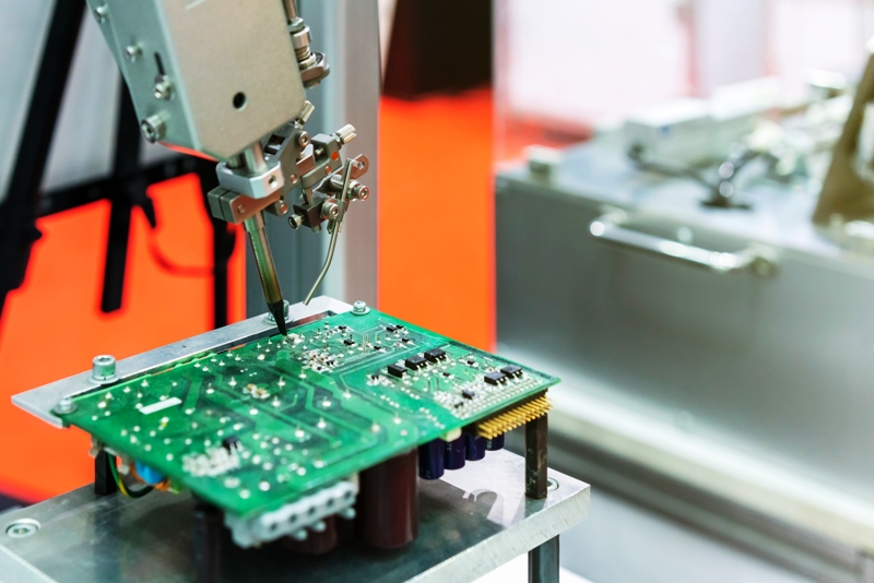
The most effective way to prevent a PCB Short Circuit is to combine several verification methods rather than relying on a single software check.
A practical verification workflow can include:
- Define PCB manufacturing requirements.
- Establish minimum clearance and routing rules.
- Configure DRC rules in the PCB design software.
- Complete PCB routing and copper pours.
- Run a complete DRC Check.
- Review critical power and signal networks manually.
- Verify via structures and internal-layer isolation.
- Perform PCB DFM Analysis.
- Review manufacturing data before Gerber release.
- Confirm final production requirements with the PCB manufacturer.
For projects that require both fabrication and assembly, early engineering review can further reduce manufacturing risks. A One-Stop PCBA Service can integrate PCB fabrication, component sourcing, assembly, inspection, and testing into a coordinated manufacturing workflow.
6. Why PCB Manufacturing Capability Matters
A PCB design is only as reliable as the manufacturing process used to produce it.
Even when a layout passes DRC, manufacturing variations can still affect trace width, spacing, hole position, copper thickness, layer registration, and other physical characteristics.
For this reason, PCB designers should consider manufacturing capability during the design stage rather than waiting until production.
Important factors include:
- Minimum line and space capability
- Mechanical and laser drilling capability
- Layer registration
- Copper plating control
- Etching accuracy
- Lamination capability
- Via fabrication
- Electrical testing
- AOI inspection
A manufacturer with appropriate process control can help identify potential production risks before fabrication begins. GOPCBA supports a broad range of PCB technologies, including multilayer PCB, HDI PCB, high-speed PCB, high-frequency PCB, heavy-copper PCB, flexible PCB, rigid-flex PCB, and controlled-impedance PCB.
7. Final Inspection and Electrical Testing
Design verification should be followed by manufacturing inspection and electrical testing.
Automated Optical Inspection (AOI) can identify defects such as:
- Open circuits
- Short circuits
- Trace width deviations
- Pattern abnormalities
- Solder mask-related defects
Electrical testing can provide another layer of protection by verifying circuit continuity and identifying unintended connections.
For complex PCBs, additional inspection technologies such as X-ray inspection may be required to evaluate hidden structures and internal connections.
GOPCBA’s quality process includes DFM checking, manufacturing process control, AOI, X-ray inspection, electrical testing, and other quality-control procedures to improve PCB production reliability.
Conclusion
Preventing a PCB Short Circuit should begin during PCB design rather than after fabrication.
Common causes include overlapping copper from different networks, insufficient clearance, overlapping vias, missing internal-layer isolation, and incorrect routing or copper-pour practices. These problems can often be reduced through properly configured PCB Design Rules, comprehensive DRC verification, careful layout inspection, and professional PCB DFM Analysis.
The most reliable approach is to combine design-rule verification with manufacturer-specific engineering review and production inspection.
By considering manufacturing requirements from the beginning, engineers can reduce redesigns, prevent avoidable PCB defects, improve production yield, and achieve more reliable electronic products.
For PCB projects ranging from prototypes to production, working with an experienced manufacturer that combines engineering review, fabrication, inspection, and assembly capabilities can provide a more controlled path from PCB design to finished product.