For hardware engineers, electrical engineers, product designers, and electronics companies, PCBA procurement is often treated as two separate workflows: PCB fabrication and component assembly. While this approach can work, it also creates additional supplier handoffs, communication gaps, BOM inconsistencies, procurement delays, and uncertainty over responsibility when a manufacturing problem occurs.
A One-Stop PCBA Service combines these activities into one coordinated manufacturing workflow. Instead of purchasing bare PCBs from one supplier and sending them to another company for component sourcing and assembly, customers can work with a single manufacturing partner from PCB design review and fabrication to component procurement, SMT/THT assembly, inspection, testing, and final delivery.
This integrated approach is particularly useful for PCB prototypes, low-volume production, NPI projects, complex SMT assemblies, medical electronics, automotive electronics, industrial controls, communication equipment, and high-volume manufacturing.
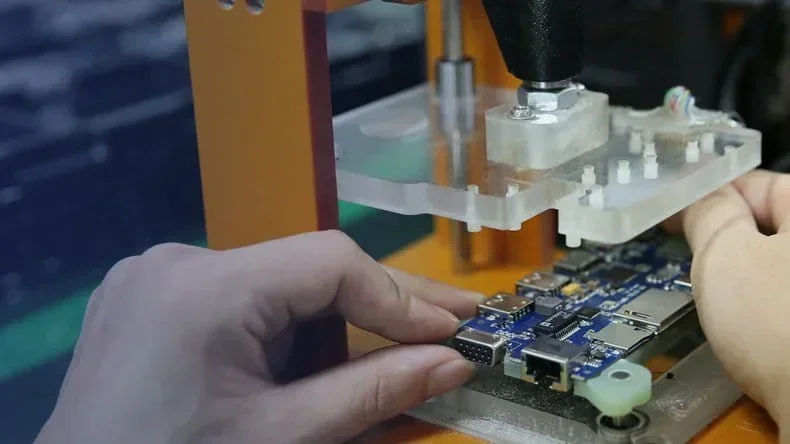
Kingda is a one-stop PCBA manufacturer integrating PCB design and development, PCB manufacturing, component procurement, SMT, DIP, finished-product assembly, and testing. The company states that it supports customers from prototype and low-volume production through high-volume manufacturing. (Kingda)
What Is One-Stop PCBA?
One-Stop PCBA refers to an integrated electronics manufacturing model in which the major stages of PCB production and assembly are managed through one manufacturing partner.
A typical workflow looks like this:
Design Review → DFM/DFA → BOM Validation → Component Procurement → PCB Fabrication → Solder Paste Printing → SMT Placement → Reflow Soldering → THT/DIP → AOI/X-Ray → ICT/FCT → Final Inspection → Packaging
The main benefit is process continuity.
Instead of coordinating:
PCB Manufacturer + Component Distributor + PCB Assembly Company + Testing Supplier + Final Assembly Supplier
a customer can work through:
One Integrated PCBA Manufacturing Partner
This reduces communication points and makes it easier to coordinate engineering changes, material sourcing, quality control, testing, and production scheduling.
Kingda describes its services as a one-stop electronics manufacturing solution, covering PCB layout, PCB manufacturing, component procurement, SMT, DIP, finished-product assembly, testing, and related engineering services. (Kingda)
The Seven Main Stages of a One-Stop PCBA Order
1. Design Review and DFM Analysis
The first stage of a professional One-Stop PCB Assembly project is engineering review.
A complete production package generally includes:
- Gerber or ODB++ files
- Bill of Materials (BOM)
- Pick-and-place / Centroid file
- Assembly drawings
- PCB stackup
- Impedance requirements
- Special process instructions
- Test requirements
The manufacturer reviews these files for consistency and manufacturability.
Common DFM problems include:
- Insufficient trace spacing
- Incorrect component footprints
- Inadequate pad dimensions
- Incorrect drill sizes
- Solder-mask clearance problems
- Insufficient component spacing
- Incorrect polarity markings
- Manufacturing structures outside supplier capability
A good DFM Review can identify these problems before materials are purchased or production begins.
Kingda provides DFM, DFA and DFX engineering support, helping customers identify potential manufacturing risks before production. (Kingda)
Why DFM Matters
A design that works electrically may still be difficult or expensive to manufacture.
For example, an engineer may choose an unusually small pad or narrow clearance to achieve a compact layout. However, if the manufacturing process cannot reliably reproduce these dimensions, the result may be low yield, solder defects, or extended production time.
This is why Design for Manufacturability should begin before the first prototype.
2. Component Procurement and BOM Validation
Component sourcing is one of the most important parts of a Turnkey PCBA project.
The supplier should review the BOM for:
- Manufacturer Part Number (MPN)
- Manufacturer
- Reference designator
- Quantity
- Package
- Availability
- Lead time
- Lifecycle status
- Approved alternatives
- Supplier information
A generic BOM description such as:
100 nF, 0402, X5R, 10 V
may be insufficient for production procurement.
A production-ready BOM should identify the exact component or clearly define acceptable alternatives.
Component Availability and Long-Lead Parts
Some components can have extended lead times or limited availability. This becomes a major issue when a PCB itself can be fabricated quickly but a critical IC cannot be sourced.
A professional PCB Component Sourcing Service should identify these risks during the BOM review rather than after PCB fabrication begins.
Kingda provides component procurement and inventory-management services supported by an ERP system. Its sourcing team states that it reviews BOM information, provides component quotations, and manages component procurement for PCBA projects. (Kingda)
Kingda also reports a dedicated component-sourcing team with more than 20 purchasing specialists and established relationships with major distributors. (Kingda)
3. PCB Fabrication
Once the design and material requirements have been confirmed, the bare PCB can be manufactured.
Typical PCB Manufacturing steps include:
Inner-Layer Imaging → Etching → Lamination → Drilling → Copper Plating → Outer-Layer Imaging → Solder Mask → Surface Finish → Electrical Testing
Depending on the product, the PCB may use:
- FR-4
- High-Tg FR-4
- High-frequency laminates
- Aluminum substrates
- Flexible polyimide materials
- Rigid-flex structures
- HDI technology
- Heavy copper
Kingda’s published PCB capabilities include standard PCB structures up to 20 layers and advanced configurations supporting significantly higher layer counts, along with HDI technologies such as microvias, stacked microvias, copper-filled microvias, and buried vias. (Kingda)
This integration between PCB Fabrication and PCB Assembly allows the manufacturer to consider assembly requirements during PCB production rather than treating fabrication and assembly as completely separate processes.
4. Solder Paste Printing and SPI
After PCB fabrication, SMT assembly begins with solder paste printing.
A stainless-steel stencil is used to deposit controlled amounts of solder paste onto the PCB pads.
Important parameters include:
- Stencil thickness
- Aperture size
- Squeegee pressure
- Printing speed
- Paste volume
- Pad geometry
- Board alignment
After printing, Solder Paste Inspection (SPI) can verify the amount and position of deposited solder paste.
Kingda’s SMT production system includes 3D SPI, AOI, X-ray, and automated SMT production lines. (Kingda)
SPI is particularly valuable because defects detected before component placement are easier and less expensive to correct.
5. SMT Component Placement
After solder paste printing, automated pick-and-place machines position components onto the PCB.
Modern SMT assembly may include:
- Resistors
- Capacitors
- Diodes
- ICs
- QFN
- QFP
- BGA
- LGA
- CSP
- PoP
- Fine-pitch components
- 0201 and 01005 passive components
Machine vision systems verify component orientation and placement accuracy.
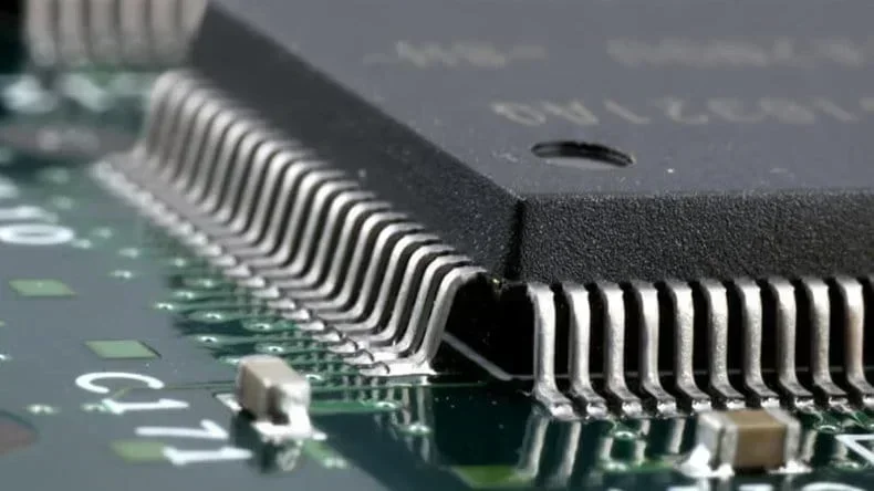
Kingda publishes support for miniature components down to 01005, BGA packages, QFN, CSP, LGA and other advanced SMT packages. Its prototype service lists 01005/0201 components, BGA down to 0.25 mm pitch, and stated IC assembly precision of ±0.03 mm under specified conditions. (Kingda)
6. Reflow Soldering and THT Assembly
Once SMT components are placed, the PCB passes through a controlled reflow soldering process.
The reflow profile must be matched to:
- Solder-paste alloy
- PCB materials
- Component thermal sensitivity
- Board thickness
- Component density
For lead-free assembly, SAC-family solder alloys are commonly used, and the thermal profile must be carefully controlled to achieve reliable solder joints without overstressing components.
For boards that contain through-hole components, THT PCB Assembly may follow SMT.
Kingda supports through-hole and mixed-technology assembly, including manual and automated insertion, wave soldering, selective soldering, press-fit assembly, and RoHS-compliant lead-free processes. (Kingda)
7. Inspection, Testing and Final Delivery
A professional One-Stop PCBA Manufacturer should provide inspection throughout the production process rather than relying only on final visual inspection.
Common inspection and testing methods include:
AOI
Automated Optical Inspection detects:
- Missing components
- Component misalignment
- Incorrect polarity
- Solder bridges
- Soldering defects
- Placement problems
X-Ray Inspection
X-ray is especially valuable for hidden solder joints such as:
- BGA
- QFN
- Bottom-terminated components
ICT
In-Circuit Testing can verify electrical connections, component characteristics, and circuit-level problems.
FCT
Functional Testing evaluates the assembled PCB under conditions closer to actual product operation.
Kingda lists AOI, X-ray, ICT, FCT, FAI, and visual inspection among its testing capabilities. (Kingda)
What Files Do You Need to Provide for One-Stop PCBA?
A complete production package significantly reduces engineering questions and production delays.
Gerber or ODB++ Files
Include:
- Copper layers
- Solder mask
- Silkscreen
- Board outline
- Drill data
For more complex projects, richer manufacturing formats such as IPC-2581 may also be considered.
BOM
A good PCB BOM should include:
- Reference designator
- Manufacturer
- Manufacturer Part Number
- Quantity
- Description
- Package
- Approved supplier
- Approved alternate
Pick-and-Place File
The centroid file should contain:
- Reference designator
- X coordinate
- Y coordinate
- Rotation
- Top/bottom information
The coordinate origin should correspond correctly to the PCB manufacturing data.
Assembly Drawing
The drawing should identify:
- Polarity
- Pin 1
- DNP components
- Special components
- Special assembly requirements
Stackup and Impedance Requirements
For high-speed PCBs, provide:
- Target impedance
- Layer information
- Trace width
- Dielectric thickness
- Copper thickness
Do not leave controlled-impedance requirements open to interpretation.
Common Problems in One-Stop PCBA Projects
BOM and Pick-and-Place Mismatches
One of the easiest ways to create assembly problems is to provide inconsistent reference designators between the BOM and centroid file.
Both should ideally be exported from the same design revision.
Component Substitution
Not every component should be substituted automatically.
Generic passive components may have acceptable alternatives, while specialized:
- RF devices
- Sensors
- Precision references
- Crystals
- Communication ICs
- Power-management devices
may require engineer approval before substitution.
Long-Lead Components
A PCB may be manufactured quickly but still wait weeks for one missing component.
Therefore, component availability should be checked before the PCB order is finalized.
Incomplete Testing Requirements
AOI does not replace functional testing.
A PCB may pass visual inspection while still having:
- Incorrect firmware
- Incorrect component value
- Functional failure
- Communication problems
- Power-system problems
When a customer requires functional testing, test specifications, fixtures, procedures, and acceptance criteria should be provided before production.
Why Choose One-Stop PCBA Manufacturing?
Reduced Supplier Coordination
A single manufacturing partner reduces communication between:
PCB Fabrication → Component Procurement → Assembly → Testing
This can make engineering changes easier to manage.
Better Accountability
When PCB manufacturing, assembly, sourcing, and testing are handled by separate companies, identifying the cause of a production problem can take longer.
With a one-stop manufacturing model, the same supplier can investigate multiple process stages.
Shorter Production Cycles
Integrated procurement and manufacturing can reduce waiting between separate suppliers.
This is particularly valuable for:
- Prototype PCB Assembly
- Quick Turn PCBA
- Low Volume PCB Assembly
- NPI
- Urgent production
Better Cost Control
A one-stop supplier can optimize:
- PCB fabrication
- Component sourcing
- Panelization
- Assembly
- Testing
- Logistics
rather than optimizing each step separately.
Kingda One-Stop PCBA Advantages
Integrated PCB and PCBA Manufacturing
Kingda integrates PCB design, PCB manufacturing, component procurement, SMT, DIP, finished-product assembly, and testing within its one-stop electronics manufacturing model. (Kingda)
Prototype-to-Mass-Production Capability
Kingda supports:
Prototype → Low Volume → Medium Volume → High Volume Production
Its published prototype service includes no MOQ, SMT/THT assembly, rapid prototyping, component sourcing, AOI/X-ray inspection, ICT/FCT, and functional testing. (Kingda)
Advanced SMT Assembly
Kingda’s published SMT capabilities include:
- 01005 components
- 0201 components
- BGA
- QFN
- CSP
- LGA
- PoP
- Double-sided SMT
- Fine-pitch assembly
- Lead-free/RoHS-compliant assembly
(Kingda)
Automated Production Lines
Kingda reports 8 fully automatic SMT production lines for high-speed and repeatable assembly. Its SMT facility also includes 3D SPI, AOI and X-ray inspection equipment. (Kingda)
Professional Component Procurement
Kingda’s component-sourcing team provides BOM review, sourcing, quotation, and inventory management. The company states that its ERP system provides real-time inventory information and supports component procurement management. (Kingda)
Comprehensive Quality Management
Kingda reports IATF 16949, ISO 13485, ISO 9001, and ISO 14001 certifications, as well as UL certification and IPC membership. (Kingda)
These quality systems are particularly relevant to projects serving automotive, medical, industrial, and other high-reliability markets.
One-Stop PCBA vs. Separate PCB and Assembly Suppliers
| Factor | One-Stop PCBA | Separate Suppliers |
|---|---|---|
| PCB fabrication | Integrated | Separate supplier |
| Component procurement | Integrated | Often separate |
| SMT/THT assembly | Integrated | Separate |
| Engineering communication | Centralized | Multiple communication channels |
| BOM management | Unified | Multiple handoffs |
| Quality responsibility | Centralized | Shared |
| Traceability | Easier to integrate | May require coordination |
| Production scheduling | Unified | Multiple schedules |
| Prototype revisions | Easier | More coordination |
| Scalability | Prototype to production | May require supplier changes |
The key advantage of the one-stop model is not simply convenience. It is process integration.
How to Make Your One-Stop PCBA Project More Efficient
1. Finalize the BOM Early
A complete BOM allows the supplier to identify sourcing problems before production.
2. Mark No-Substitution Components
Clearly identify components that must use a specific MPN.
3. Provide Complete Manufacturing Files
Use a consistent design revision for:
Gerber + BOM + Centroid + Assembly Drawing + Stackup
4. Define Testing Requirements Before Production
Specify whether your project requires:
AOI, X-Ray, ICT, FCT, Programming, Burn-In, or Environmental Testing
5. Design for Manufacturing
Work with the manufacturer during the design phase instead of waiting until after the first prototype fails.
Conclusion
A One-Stop PCBA Service can simplify the complete electronics manufacturing process by combining PCB fabrication, component sourcing, SMT/THT assembly, inspection, testing, and final assembly within one coordinated workflow.
The most important advantage is not simply having fewer suppliers. It is the ability to connect engineering data, materials, manufacturing processes, quality control, and testing into a more consistent production system.
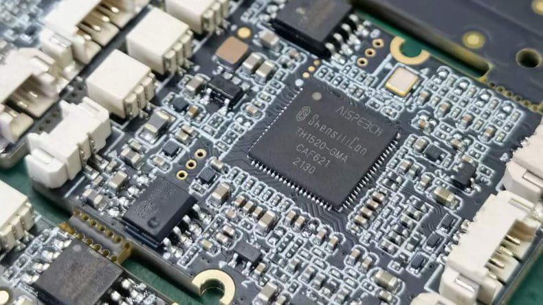
For hardware developers, the ideal one-stop manufacturing partner should be able to support the entire product lifecycle:
Kingda provides this integrated manufacturing model, with published capabilities covering PCB fabrication, component procurement, SMT, THT/DIP, rapid prototyping, low-volume production, high-volume PCBA, AOI, SPI, X-ray, ICT, FCT, and finished-product assembly. (Kingda)
For companies looking to reduce supplier handoffs while maintaining engineering control, quality consistency, and production scalability, Kingda One-Stop PCBA Manufacturing provides an integrated path from prototype development to production.