
PCB Solder Mask and Gerber Files: Complete Design Guide
In PCB manufacturing, solder mask coverage is an important part of the final board appearance, electrical insulation, and assembly performance. One common misunderstanding is that selecting an option such as “via tenting” or “via opening” when placing an order can change the solder mask requirements of the PCB.
In practice, the PCB Solder Mask requirements should already be defined in the design data before manufacturing begins. The Gerber output contains the graphical information that determines where solder mask is present and where openings are required.
Therefore, the ordering options provided by a manufacturer should be treated as confirmation of the intended manufacturing requirements rather than a replacement for the design files.
For projects with demanding fabrication requirements, working with an experienced PCB Manufacturing partner can help ensure that design data, manufacturing requirements, and production processes remain consistent.
Gerber files are standardized manufacturing data generated from PCB design files. Unlike the original PCB design database, Gerber files primarily describe the final graphical information required to manufacture each PCB layer.
A typical Gerber package may contain data for: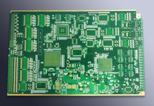
- Copper layers
- Solder mask layers
- Silkscreen layers
- Paste layers
- Board outline
- Other manufacturing-related layers
Among these files, the solder mask layers are particularly important when determining whether specific PCB areas should be covered by solder mask or left exposed.
The solder mask layer uses graphical information to define areas where solder mask openings are required.
In simple terms:
- A corresponding opening in the solder mask layer indicates that the underlying area is intended to remain exposed.
- No corresponding opening indicates that the area is intended to remain covered by solder mask.
This means that Gerber Files provide the actual graphical manufacturing information used to interpret the final solder mask pattern.
For example, if a via is intentionally designed to have a solder mask opening, the corresponding solder mask Gerber layer should contain the required opening around that via.
If the via is intended to be covered, the solder mask data should not contain an opening at that location.
A common question is: if the customer selects “via tenting” during ordering but the Gerber file shows an opening, why can’t the manufacturer simply modify the file?
The main reason is that the manufacturer cannot reliably determine the original design intent from an ordering option alone.
Consider a PCB where several vias are intentionally opened because they are used as test points, grounding structures, thermal interfaces, or other functional features.
If a manufacturer sees an order option requesting via tenting and automatically removes the openings from the Gerber file, an intentional design feature could be incorrectly changed.
The opposite situation can also occur. A designer may accidentally generate an opening in the solder mask layer while intending the via to remain covered.
Without confirmation from the design owner, the manufacturer cannot safely determine whether the Gerber data or the ordering instruction represents the actual engineering requirement.
This is why the final manufacturing data should accurately reflect the designer’s intended configuration.
Manufacturing companies generally rely on the released production files as the primary technical reference.
Changing critical production data without updating the corresponding design files can create several problems:
- The manufactured PCB may no longer match the original design.
- Future revisions may use incorrect source data.
- Engineering teams may misunderstand the intended solder mask configuration.
- Manufacturing and assembly teams may work from inconsistent information.
- Quality disputes may become difficult to resolve.
For complex boards, early engineering review is especially important. GOPCBA provides PCB Capabilities information covering solder mask registration, minimum solder mask dam, HDI structures, copper features, and other manufacturing parameters that can be considered during PCB design.
The difference between via tenting and solder mask opening is important when preparing PCB manufacturing data.
A tented via is covered by solder mask on the corresponding PCB surface.
Via tenting is commonly used when there is no need for direct access to the via pad. Covering the via can help protect the copper surface from environmental exposure and can reduce the possibility of unwanted solder entering the via during assembly.
However, the appropriate treatment depends on the PCB design, via structure, assembly process, and application requirements.
A solder mask opening leaves a defined conductive area exposed.
An opening may be required for:
- Test points
- Electrical contacts
- Certain thermal structures
- Specific grounding features
- Components requiring exposed copper
- Other functional PCB features
The designer should therefore define these requirements in the PCB design rather than relying solely on an order-form selection.
Preventing solder mask problems is relatively straightforward when the design process includes a systematic verification procedure.
Before generating manufacturing files, determine which vias and pads should be covered and which should remain exposed.
For example:
- Standard vias may be designed with tenting.
- Test points may require solder mask openings.
- Certain thermal or grounding structures may require exposed copper.
- Component pads normally require openings according to the PCB footprint and assembly requirements.
The exact configuration should be established in the PCB design software.
Do not assume that the exported Gerber files perfectly match the original PCB design without checking them.
After exporting the files, open the Gerber data in an appropriate viewer and inspect the solder mask layers.
Check whether:
- Required via openings are present.
- Unwanted via openings are absent.
- Pad openings have the correct dimensions.
- Solder mask dams are maintained between adjacent pads.
- The solder mask pattern matches the copper and component layout.
This step is especially important for fine-pitch components, high-density PCB layouts, HDI boards, and designs with closely spaced vias.
The final Gerber package should be compared against the released PCB design.
If a discrepancy is discovered, the preferred approach is to correct the original design and regenerate the manufacturing files.
Do not attempt to solve a design-data problem simply by changing an ordering option.
Solder mask accuracy is influenced not only by the PCB design but also by the manufacturing process.
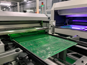
Important manufacturing factors include:
- Solder mask registration
- Minimum solder mask dam
- Pad dimensions
- Copper-to-copper spacing
- Via structure
- Board thickness
- Surface finish
- Layer registration
- Imaging accuracy
For example, a high-density PCB may require smaller solder mask dams and tighter registration tolerances than a conventional board.
Therefore, designers should understand the manufacturer’s capabilities before finalizing the PCB layout.
GOPCBA’s manufacturing capabilities include controlled solder mask registration and minimum solder mask dam specifications, helping engineers evaluate whether their design requirements are suitable for production.
The importance of accurate Gerber data does not end with bare PCB fabrication.
The PCB manufacturing files are also closely related to downstream assembly. Incorrect solder mask openings can affect solder deposition, component soldering, exposed copper areas, and the overall assembly process.
For example, incorrect solder mask dimensions around fine-pitch component pads can influence solder bridging and solder joint quality.
GOPCBA provides PCB Assembly services covering prototype, low-volume, and mass-production requirements, together with engineering support for DFM review and Gerber file verification.
For projects that will proceed directly from PCB fabrication to SMT assembly, Gerber verification should be completed before production.
The manufacturing team should confirm that:
- PCB dimensions are correct.
- Solder mask openings match the component footprints.
- Pad geometry is correct.
- Via treatment is consistent with the design.
- Surface finish requirements are correctly specified.
- Assembly-related PCB features are suitable for the intended process.
For SMT projects, GOPCBA also accepts Gerber, BOM, and Pick & Place files as part of the production preparation process.
The fundamental principle of PCB fabrication is simple: the manufacturer produces the board according to the released manufacturing data.
The original PCB design establishes the engineering intent, while the exported manufacturing files translate that intent into production-ready information.
For this reason, designers should not treat Gerber generation as a simple export operation. It should be considered an important stage of the engineering verification process.
A recommended workflow is:
- Complete the PCB layout.
- Define via and solder mask requirements.
- Verify pad and via properties.
- Run design-rule checks.
- Generate Gerber files.
- Inspect the solder mask layers.
- Compare Gerber files with the original PCB design.
- Confirm manufacturing requirements.
- Release the final production package.
- Submit the verified files for PCB fabrication.
Before submitting PCB files for manufacturing, engineers can use the following checklist:
- Are all required solder mask openings present?
- Are unintended via openings removed?
- Are test points correctly exposed?
- Are component pads correctly opened?
- Is the solder mask dam sufficient between adjacent pads?
- Does the solder mask layer match the copper layer?
- Do the Gerber files match the latest PCB design revision?
- Are via tenting requirements clearly defined?
- Are manufacturing capabilities compatible with the design?
- Have all final production files been reviewed?
If any discrepancy exists between the design requirement and the exported manufacturing files, the design should be corrected and the Gerber package regenerated before production.
PCB Solder Mask coverage is not simply an option selected during the PCB ordering process. It is a design requirement that must be accurately represented in the final manufacturing data.
Gerber Files provide the graphical information used to define solder mask openings and covered areas. Whether a via is tented or opened should therefore be determined during PCB design and verified after Gerber generation.
The most reliable approach is to maintain consistency between the PCB source design, Gerber files, manufacturing requirements, and assembly requirements.
By carefully checking solder mask layers before fabrication and working with a manufacturer that provides engineering and DFM support, designers can reduce manufacturing errors, avoid unnecessary revisions, and improve PCB production reliability.
For projects requiring fabrication and assembly from a single manufacturing partner, GOPCBA provides One-Stop PCBA Manufacturing covering PCB fabrication, component sourcing, PCB assembly, testing, and related engineering services.