What Is AOI Inspection? Complete PCB Inspection Guide
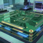
AOI inspection, or Automated Optical Inspection, is an important quality-control technology used throughout modern electronics manufacturing. It uses cameras and image-processing algorithms to inspect PCBs and PCB assemblies for visible manufacturing defects.
Unlike manual visual inspection, an AOI Inspection system can automatically compare the actual PCB image with predefined design or inspection criteria. When a potential defect is identified, the system flags the location for further review.
AOI is widely used in SMT manufacturing because it can quickly inspect large numbers of solder joints, components, and PCB patterns while maintaining consistent inspection standards.
However, AOI does not electrically power the PCB and therefore cannot detect every possible component or circuit defect. For this reason, AOI is normally combined with other inspection and testing methods such as X-ray inspection, ICT, flying probe testing, and functional testing.
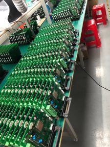
For PCB fabrication, GOPCBA also integrates automated inspection into its broader PCB Manufacturing quality-control process.
Automated Optical Inspection uses cameras, lighting systems, image-processing software, and predefined inspection parameters to examine a PCB or assembled PCBA.
Depending on the equipment and application, AOI systems may use 2D imaging or advanced 3D inspection technologies.
The basic process typically includes:
- Positioning the PCB or PCBA in the inspection system.
- Capturing high-resolution images of the board.
- Identifying components, solder joints, pads, and PCB features.
- Comparing the captured information against programmed inspection criteria.
- Identifying deviations or suspected defects.
- Marking defect locations for operator or engineering review.
- Recording inspection results for process monitoring and quality control.
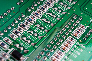
Modern AOI systems can inspect component placement, solder joints, polarity, solder bridges, missing components, and other visible manufacturing conditions.
Depending on the system configuration and inspection stage, AOI can identify defects such as:
- Missing components
- Incorrect component placement
- Component misalignment
- Incorrect polarity
- Tombstoning
- Insufficient solder
- Excessive solder
- Solder bridges
- Solder shorts
- Open solder connections
- Abnormal solder-joint geometry
- PCB pattern abnormalities
GOPCBA’s published PCBA inspection capabilities include AOI inspection for wrong parts, missing parts, wrong polarity, misalignment, tombstoning, solder shorts, solder bridges, and cold solder conditions.
PCB assemblies contain hundreds or even thousands of components and solder connections. Manually inspecting every connection at production speed is difficult and can result in inconsistent inspection quality.
PCB Inspection using AOI provides several advantages.
Faster Inspection
AOI can inspect large numbers of components and solder joints quickly, making it suitable for automated SMT production lines.
This allows manufacturers to identify defects earlier instead of waiting until final assembly or functional testing.
Consistent Inspection Criteria
Manual inspection can vary depending on operator experience, fatigue, lighting conditions, and workload.
AOI uses programmed inspection criteria to provide a more consistent inspection process.
Early Defect Detection
Finding defects as early as possible reduces the cost of rework.
For example, if an incorrect solder paste print is identified immediately after printing, the problem can be corrected before components are placed and soldered.
This prevents the same defect from propagating through later production stages.
Process Data Collection
AOI systems can generate inspection data that helps engineers identify recurring production problems.
If the same defect repeatedly appears in a particular location, engineers can investigate potential causes such as:
- Stencil design
- Solder paste printing
- Component placement
- Reflow profile
- PCB pad design
- Component orientation
- Equipment calibration
This makes AOI more than a final inspection tool. It can also support continuous SMT process improvement.
The location of AOI equipment in the production line affects the type of defects that can be detected and the value of the inspection.
Three common inspection points are after solder paste printing, before reflow soldering, and after reflow soldering.
Solder paste printing is the first major SMT process that can introduce assembly defects.
Typical problems include:
- Insufficient solder paste
- Excessive solder paste
- Offset solder paste deposits
- Incorrect solder paste volume
- Solder paste bridging between pads
If these problems are detected before component placement, the production team can correct the printing process before additional manufacturing stages are performed.
For advanced SMT production, Solder Paste Inspection (SPI) can provide dedicated inspection of solder paste volume, position, and distribution.
GOPCBA’s SMT capabilities include SMT PCB Assembly with SPI, AOI, X-ray, and automated SMT production equipment.
Another inspection point is after components have been placed onto solder paste but before the PCB enters the reflow oven.
At this stage, AOI can help identify:
- Missing components
- Incorrect component placement
- Component rotation
- Incorrect polarity
- Placement offsets
- Other visible placement defects
Detecting these problems before reflow can reduce unnecessary soldering defects and help engineers correct problems with the pick-and-place process.
This inspection stage can also provide useful process data for machine calibration and placement optimization.
Post-reflow inspection is one of the most common AOI applications in SMT manufacturing.
After reflow, AOI can inspect the completed solder joints and identify defects resulting from:
- Solder paste printing
- Component placement
- Reflow soldering
- Component orientation
- Solder volume
- PCB pad conditions
Post-reflow AOI provides a final automated visual inspection before the assembly moves to subsequent testing or production stages.
Although AOI is highly effective for visual inspection, it cannot detect every type of PCB or PCBA defect.
The main limitation is that AOI primarily evaluates visible physical characteristics. It does not directly verify all electrical functions of a circuit.
For example, AOI may not reliably detect:
- Hidden BGA solder-joint defects
- Internal PCB connections
- Certain component failures
- Incorrect electrical values
- Functional circuit failures
- Some intermittent electrical problems
Therefore, PCB Testing should normally combine multiple inspection technologies based on the product’s complexity and reliability requirements.
X-ray inspection can examine structures that are not visible from the surface.
It is particularly useful for:
- BGA solder joints
- Hidden solder connections
- Via-in-pad structures
- Internal PCB features
- Voids in solder joints
- Complex multilayer assemblies
GOPCBA provides X-ray inspection as part of its PCBA quality-control capabilities, alongside AOI, ICT, FCT, and other testing methods.
In-Circuit Test (ICT) evaluates electrical characteristics through dedicated test points.
Depending on the system, ICT can identify problems involving:
- Open circuits
- Short circuits
- Component values
- Circuit connections
- Certain assembly defects
AOI and ICT therefore examine different aspects of the same PCBA.
AOI primarily focuses on visual and physical conditions, while ICT provides electrical verification.
Functional testing verifies whether the assembled product operates according to its intended functional requirements.
For example, a functional test may evaluate:
- Power-up behavior
- Communication interfaces
- Sensor response
- Display output
- Motor operation
- Signal transmission
- User-interface functions
A PCBA may pass AOI while still having an electrical or functional problem, which is why functional testing can be necessary for complex electronic products.
Each inspection technology has a different purpose.
| Inspection Method | Primary Purpose |
|---|---|
| AOI | Visual inspection of PCB patterns, components, and solder joints |
| SPI | Inspection of solder paste volume and position |
| X-Ray | Inspection of hidden solder joints and internal structures |
| ICT | Electrical verification of circuits and components |
| Flying Probe | Fixtureless electrical testing |
| Functional Test | Verification of actual product operation |
| Manual Inspection | Visual confirmation and defect review |
A professional manufacturing process should select the appropriate combination according to PCB complexity, component density, production volume, and reliability requirements.
As PCB assemblies become smaller and more complex, automated inspection becomes increasingly important.
Modern SMT production may involve:
- 01005 components
- Fine-pitch QFP
- QFN
- BGA
- CSP
- LGA
- Double-sided SMT
- High-density component placement
These packages create greater challenges for manual inspection.
AOI can inspect a large number of components and solder joints while maintaining repeatable inspection criteria.
For complex assemblies, however, AOI should be combined with X-ray and electrical testing rather than used as the only quality-control method.
AOI works most effectively when integrated into a complete quality-management system.
A typical PCBA quality-control flow may include:
IQC → SPI → SMT/THT Assembly → AOI → X-Ray → ICT/FCT → Final Inspection
Each stage addresses different manufacturing risks.
Incoming Material Inspection
Before assembly begins, PCBs, components, solder materials, and other production materials should be checked against approved manufacturing documentation.
Process Inspection
During production, SPI, AOI, and other inspection methods monitor manufacturing quality and help identify process deviations.
Electrical Testing
ICT, flying probe, and functional testing verify electrical connectivity and product performance.
Final Inspection
Final inspection confirms that the completed PCBA meets the customer’s defined appearance, assembly, labeling, packaging, and quality requirements.
GOPCBA describes a quality-control flow covering incoming inspection, SPI, SMT/THT assembly, AOI, X-ray, ICT/FCT, and outgoing quality control.
AOI is useful across different stages of product development.
Prototype Production
During prototype production, AOI can help engineers identify design-related or assembly-related issues early.
Because prototype quantities are usually smaller, inspection data can also be used to improve the PCB layout, component footprint, stencil design, and assembly process before volume production.
Low-Volume Production
For low-volume products, AOI provides automated inspection without relying entirely on manual visual inspection.
This is especially valuable for products with frequent engineering changes.
High-Volume Production
In high-volume manufacturing, AOI becomes even more important because manual inspection alone cannot efficiently maintain consistent inspection coverage across large production quantities.
Automated inspection helps manufacturers monitor process stability and identify recurring defects.
AOI performance depends not only on the inspection equipment but also on PCB design and manufacturing preparation.
Optimize PCB Footprints
Component footprints should provide sufficient pad geometry and spacing for reliable soldering and inspection.
Poor footprint design can create false AOI alarms or make genuine defects more difficult to identify.
Maintain Accurate Manufacturing Data
The AOI program needs accurate component and PCB information.
Manufacturing data should remain consistent across:
- Gerber files
- BOM
- Pick-and-place files
- Assembly drawings
- Component polarity
- Reference designators
GOPCBA’s quality-management process includes pre-production verification of PCB specifications, BOM information, component designators, pick-and-place files, and special testing requirements.
Control the SMT Process
AOI should not be used simply to detect defects after they occur.
Inspection data should be fed back into the SMT process to identify root causes.
For example, repeated solder bridges may indicate problems with:
- Stencil aperture design
- Solder paste volume
- Pad spacing
- Printing alignment
- Reflow parameters
Process feedback can therefore improve production yield over time.
GOPCBA integrates AOI into its broader PCB assembly inspection and testing process.
Its published PCBA capabilities include AOI inspection for component presence, incorrect parts, polarity, placement, tombstoning, solder shorts, solder bridges, and cold solder conditions. It also supports X-ray, ICT, functional testing, FAI, and other reliability tests.
For customers requiring complete manufacturing and assembly, One-Stop PCBA Services can integrate PCB fabrication, component sourcing, SMT/THT assembly, inspection, testing, and final delivery into one coordinated workflow.
This approach reduces unnecessary supplier handoffs and makes it easier to maintain consistency between engineering data, production processes, inspection requirements, and final testing.
Before starting PCB assembly, manufacturers and engineers should confirm the following:
- Are the Gerber files complete and correct?
- Is the BOM accurate and up to date?
- Are component reference designators correct?
- Are component polarities clearly defined?
- Is the pick-and-place file accurate?
- Are PCB footprints suitable for SMT assembly?
- Are solder paste requirements clearly defined?
- Are inspection criteria configured correctly?
- Is AOI performed at the appropriate production stage?
- Are X-ray inspection requirements defined for hidden solder joints?
- Are ICT or functional testing requirements defined?
- Are inspection results recorded for quality traceability?
A complete inspection strategy helps prevent defects from progressing from one manufacturing stage to another.
AOI Inspection is an essential quality-control technology for modern PCB assembly. By using cameras and automated image analysis, AOI can quickly identify many visible PCB and soldering defects, including missing components, misalignment, polarity errors, solder bridges, insufficient solder, and other assembly problems.
However, AOI should not be considered a replacement for all other testing methods.
The most reliable approach combines Automated Optical Inspection, SPI, X-ray, ICT, flying probe testing, functional testing, and final inspection according to the specific requirements of the PCBA.
For high-density SMT assemblies and high-reliability electronic products, integrating SMT Inspection into a complete manufacturing quality system can significantly improve defect detection, process control, production consistency, and product reliability.
GOPCBA supports PCB fabrication, SMT/THT assembly, AOI, X-ray, ICT/FCT, and other inspection and testing processes, providing an integrated approach to PCB Testing from prototype through production.