PCB Gold Fingers: Design, Manufacturing and DFM Guide
Gold-plated contact pads along the edge of computer memory modules, graphics cards, expansion cards, and other electronic boards are commonly known as gold fingers. In the PCB industry, these contacts are also referred to as PCB Gold Fingers or edge connectors.
Gold fingers provide a reliable electrical and mechanical interface between a PCB and a mating connector. Because they may be inserted and removed repeatedly, their design requires special attention to contact geometry, plating, edge beveling, solder mask openings, copper routing, and manufacturing tolerances.
This guide explains the primary applications of gold fingers, key Gold Finger Design requirements, manufacturing considerations, and methods for improving production reliability.
Gold fingers are exposed conductive contacts located along the edge of a PCB. They allow one PCB to connect directly to a slot or connector without requiring a separate wire connection.
PCB-to-Board Interconnection
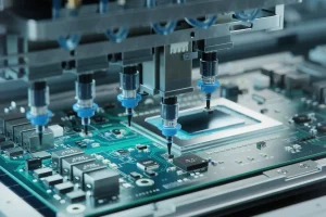
A daughterboard or expansion card can be inserted into a mating connector on a motherboard. The gold fingers establish electrical connections between the two boards and transmit power, control signals, and high-speed data.
Common examples include:
- Computer memory modules
- Graphics cards
- Sound cards
- Network interface cards
- Expansion cards
- Industrial control boards
- Embedded computing modules
For these applications, the gold finger area must maintain reliable electrical contact while withstanding repeated insertion and removal.
Functional Expansion Interfaces
Gold fingers are widely used when a secondary PCB needs to connect to a primary PCB through a card-edge connector.
Compared with permanently soldered connections, this structure allows the secondary board to be installed, removed, upgraded, or replaced more easily.
This makes the PCB Edge Connector an important interface for modular electronic systems.
External Device Connections
Edge connectors can also be used as part of external or internal interfaces for electronic equipment.
Depending on the application, PCB edge contacts may carry:
- Digital signals
- High-speed data
- Power
- Ground
- Control signals
- Audio or video signals
The electrical and mechanical requirements depend on the connector design and intended operating environment.
A reliable Gold Finger PCB requires more than simply applying gold plating to the board edge. The PCB layout and manufacturing structure must be designed specifically for edge-connector applications.
Gold Finger Beveling
A beveled PCB edge allows the board to enter the mating connector more smoothly.
The bevel angle is commonly around 30° or 45°, depending on the board and connector requirements. The exact bevel geometry should be confirmed according to the connector specification and PCB thickness.
Designers should also maintain sufficient clearance between the gold finger area and the board edge.
If the gold fingers are positioned too close to the edge, the beveling process may remove part of the contact area.
For reliable production, the PCB outline, board thickness, bevel angle, and gold finger length should therefore be considered together.
GOPCBA supports a wide range of PCB fabrication technologies and manufacturing requirements. Its PCB Manufacturing capabilities can be evaluated during the early design stage to ensure that gold finger requirements are compatible with the selected manufacturing process.
Without an appropriate bevel, the sharp edge of the PCB can interfere with the connector during insertion.
A properly designed bevel helps:
- Reduce insertion resistance
- Protect connector contacts
- Reduce mechanical damage
- Improve insertion consistency
- Extend connector service life
The board corners may also require additional edge treatment to prevent sharp corners from damaging the mating connector.
The gold finger area normally requires a complete solder mask opening because the exposed contacts must directly engage with the mating connector.
If solder mask covers the contact area, repeated insertion and removal can damage the solder mask and interfere with electrical contact.
Therefore, solder mask design is an important part of Gold Finger Design.
Recommended Solder Mask Considerations
The solder mask opening should be designed according to the gold finger geometry and manufacturer’s capabilities.
Designers should verify:
- Solder mask opening width
- Clearance from the gold finger edge
- Clearance between the opening and surrounding copper
- Minimum solder mask dam
- Distance between vias and gold fingers
- Board edge tolerance
The exact values should always be confirmed with the PCB manufacturer because manufacturing capabilities vary.
Keep Vias Away From the Gold Finger Area
Vias located too close to gold fingers can create several manufacturing and reliability concerns.
Unless specifically required by the design, vias should generally be kept away from the gold finger contact area. If a via is positioned too close to the contact region, solder mask opening, plating, beveling, or mechanical processing may affect the final contact structure.
The PCB edge should be designed to support smooth insertion into the mating connector.
Sharp corners can interfere with connector insertion and may cause unnecessary mechanical stress.
Edge Bevel or Corner Treatment
Depending on the connector design, the board edge may use a bevel, chamfer, or other corner treatment.
The objective is to create a smooth insertion path while maintaining sufficient mechanical strength.
For gold finger boards, the final board outline should be reviewed together with the beveling process before manufacturing data is released.
Copper routing near the gold finger area requires special attention.
In general, unnecessary copper pours should be avoided around the exposed contact region.
If multiple gold fingers belonging to the same network are connected through an inappropriate copper pour, they may become electrically and physically connected in a way that changes the intended contact structure.
Each gold finger should maintain the required individual geometry unless the electrical design specifically requires a common connection.
Gold Finger Lead Routing
The traces connecting gold fingers to the internal PCB circuitry should transition smoothly into the board.
Depending on the design, angled or rounded routing may be preferable to abrupt 90-degree transitions, particularly where the trace approaches the edge of the board.
Designers should also maintain appropriate spacing between adjacent traces and between the gold finger leads and other copper features.
For advanced PCB projects, GOPCBA provides PCB Capabilities information that can help engineers evaluate trace/space, board thickness, copper, drilling, plating, and other production requirements before releasing the design.
Some edge connector designs use gold fingers with different lengths.
Long and short contacts can create a controlled connection sequence when the PCB is inserted into the connector.
For example, longer contacts may establish ground or other required connections before shorter signal contacts become fully engaged.
Key Design Considerations
When designing long and short gold fingers, engineers should carefully define:
- Contact length
- Lead length
- Lead width
- Clearance between leads
- Gold finger spacing
- Transition geometry
- Distance from the board edge
The exact dimensions should be determined from the mating connector specification rather than applying one universal value to every PCB.
Where a lead must transition from the gold finger into the main PCB routing area, a smooth angled or curved transition can help avoid unnecessary mechanical and manufacturing problems.
Panelization requires additional attention when manufacturing PCBs with edge connectors.
Gold fingers must remain accessible for the plating and beveling processes, while the panel structure must provide sufficient mechanical stability during fabrication.
Small Gold Finger Boards
For small boards, the manufacturing process may require special panelization and routing arrangements.
The panel design should consider:
- Board orientation
- Gold finger direction
- Tooling holes
- Routing position
- Beveling access
- Plating bus requirements
- Final board separation
The gold finger area should be positioned to allow the required plating and mechanical processes to be performed without damaging the contact surface.
Gold Fingers Facing the Panel Interior
When possible, gold finger boards can be arranged so that the gold finger area is oriented appropriately within the manufacturing panel.
This can simplify the addition of plating connections and improve process efficiency.
Panelization should always be reviewed with the PCB manufacturer before production, particularly for small boards, unusual outlines, or boards requiring edge beveling.
Manufacturing a gold finger PCB involves more than standard PCB fabrication.
A typical production workflow may include:
- Material preparation
- Inner-layer imaging
- Inner-layer etching
- Inner-layer inspection
- Lamination
- Drilling
- Copper deposition
- Pattern plating
- Outer-layer imaging
- Outer-layer etching
- Solder mask application
- Solder mask imaging
- Silkscreen
- Surface finishing
- Gold finger plating
- PCB routing
- Edge beveling
- Electrical testing
- Final inspection
- Packaging and shipment
The actual process sequence varies depending on the PCB structure, surface finish, plating requirements, and manufacturer.
For high-reliability applications, process control is particularly important because gold fingers are directly exposed to mechanical wear during repeated connector insertion.
CAM engineering plays an important role in converting PCB design data into production-ready manufacturing data.
For boards containing gold fingers, the CAM process may need to account for:
- Plating thickness
- Trace compensation
- Gold finger dimensions
- Edge clearance
- Board thickness tolerance
- Bevel geometry
- Plating bus structures
- Panelization requirements
The final compensation values depend on the manufacturer’s process capabilities and the required finished dimensions.
Gold Finger Lead Compensation
Gold finger leads and contact pads may require specific treatment during CAM preparation.
Engineers should verify whether the selected plating process requires compensation of the gold finger geometry and associated copper features.
The objective is to ensure that the finished gold finger dimensions remain within the required tolerance after plating and subsequent processing.
Two commonly discussed gold surface finishes are hard gold plating and ENIG.
Hard Gold Plating
Hard gold plating is commonly used for PCB edge connectors because the gold layer is designed to withstand repeated mechanical contact.
It offers:
- Good wear resistance
- Good electrical conductivity
- Corrosion resistance
- Long contact life
- Suitability for repeated insertion
Because hard gold plating is more expensive than conventional surface finishes, it is normally applied selectively to areas such as gold fingers rather than across the entire PCB.
ENIG Surface Finish
ENIG, or Electroless Nickel Immersion Gold, provides a flat and solderable surface and is widely used for component pads, BGA areas, and other PCB features.
It can also be considered for certain edge-contact applications where high mechanical wear resistance is not the primary requirement.
However, ENIG and hard gold are not interchangeable in every gold finger application. The appropriate finish should be selected according to insertion cycles, contact force, electrical requirements, and connector specifications.
Because gold finger PCBs often involve additional plating and mechanical processes, design verification should be completed before production.
A professional PCB DFM Analysis can help identify potential manufacturing problems before the design reaches production.
Typical inspection areas may include:
- Gold finger dimensions
- Edge clearance
- Solder mask openings
- Via locations
- Trace spacing
- Board outline
- Bevel requirements
- Plating structures
- Drill locations
- Panelization
- Manufacturing tolerances
Why DFM Review Is Important
Gold finger PCBs can be more expensive than standard boards because they may require special plating, beveling, and additional processing.
If a manufacturing problem is discovered only after production, the cost of rework or scrap can be significant.
Early DFM review helps identify potential problems while design changes are still relatively inexpensive.
After manufacturing, the gold finger area should be carefully inspected.
Important inspection items include:
- Gold plating appearance
- Plating coverage
- Contact surface condition
- Gold finger dimensions
- Edge bevel quality
- Scratches and contamination
- Copper exposure outside intended areas
- Board edge condition
- Electrical continuity
For boards intended for frequent insertion and removal, mechanical durability is just as important as electrical performance.
Depending on the application, manufacturers may also perform dimensional inspection, electrical testing, automated optical inspection, or other quality-control procedures.
For projects that require both fabrication and assembly, integrating PCB production with downstream assembly can simplify quality management. GOPCBA provides PCB Assembly Services for projects requiring a coordinated PCB manufacturing and assembly workflow.
Before releasing a Gold Finger PCB for production, engineers should review the following items:
- Are the gold finger dimensions correct?
- Is the edge bevel compatible with the connector?
- Is the gold finger area completely free of unnecessary solder mask?
- Are vias sufficiently far from the gold finger region?
- Are adjacent contacts electrically isolated?
- Is the copper routing correctly designed?
- Are long and short fingers correctly dimensioned?
- Is the board outline compatible with beveling?
- Is panelization suitable for gold plating?
- Are plating bus connections properly designed?
- Is the selected gold finish suitable for the required insertion cycles?
- Are the board thickness and edge tolerances compatible with the connector?
- Have the manufacturing files been checked?
- Has DFM analysis been completed?
PCB Gold Fingers are critical mechanical and electrical interfaces used in memory modules, expansion cards, industrial electronics, embedded systems, and other modular PCB applications.
Reliable gold finger performance depends on much more than the gold plating itself. The complete design must consider beveling, solder mask openings, copper routing, via placement, long and short contact geometry, panelization, plating, CAM compensation, and final inspection.
The most effective approach is to evaluate these requirements during the PCB design stage and verify them before manufacturing.
By combining accurate Gold Finger Design, appropriate surface finishing, professional manufacturing processes, and DFM verification, engineers can improve connector reliability, reduce manufacturing risks, and achieve consistent performance over repeated insertion cycles.
For production-ready Gold Finger PCB projects, selecting an experienced manufacturer with appropriate PCB Manufacturing capabilities, plating processes, engineering support, and quality-control systems can help ensure that the finished board meets both electrical and mechanical requirements.