PCB Panelization: 10 Key Design Considerations
When completing a PCB design, some boards need to be arranged into a larger manufacturing panel before production. This process is known as PCB panelization. But when is panelization necessary, and what should engineers consider when designing a panel?
Proper PCB panelization design can directly affect manufacturing efficiency, assembly quality, material utilization, and overall production cost. For projects that require automated assembly or multiple small boards, a well-designed panel can make the entire manufacturing process more efficient.
Why Is PCB Panelization Necessary?
PCB panelization involves combining multiple individual PCB units into a single larger panel for manufacturing and assembly. Instead of producing and handling each small PCB separately, manufacturers can process several boards together.
There are three common reasons for using PCB panelization:
1. Meeting manufacturing requirements
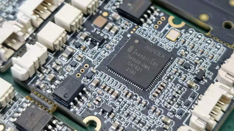
Some PCBs are too small to be securely handled by manufacturing equipment or fixtures. Combining multiple small boards into one panel provides sufficient size for automated production and handling.
2. Improving SMT assembly efficiency
Multiple PCB units can pass through the SMT production line as one panel. This reduces repeated loading and handling operations and can significantly improve production efficiency.
For projects requiring automated component placement, solder paste printing, and reflow soldering, proper panel design is an important part of the overall SMT assembly process. GOPCBA provides comprehensive SMT PCB Assembly services for prototype, low-volume, and production requirements.
3. Improving material utilization
Some PCBs have irregular shapes that may leave unused areas on a production sheet. Proper panelization can arrange these boards more efficiently, reduce material waste, and help lower manufacturing costs.
What Are the Common PCB Panelization Methods?
Different PCB shapes and manufacturing requirements require different panel connection methods. The three common methods are V-Cut, stamp holes, and hollow connection tabs.
1. V-Cut Panelization
V-Cut, also known as V-scoring, creates a V-shaped groove between adjacent PCB units. The remaining material is thin enough to allow the individual boards to be separated after manufacturing.
V-Cut is particularly suitable for regular rectangular or square PCBs because the scoring line must generally remain straight. It is not suitable for curved or highly irregular board outlines.
When using V-Cut, sufficient clearance should be maintained between components and the scoring line. A clearance of more than 0.5 mm is commonly used to prevent interference between components and the cutting tool.
For reliable PCB manufacturing, the V-Cut position should be clearly defined in the fabrication data so that the manufacturer can correctly identify the separation lines.
2. Stamp Hole Panelization
Stamp holes are widely used for irregularly shaped PCBs where V-Cut cannot follow the board outline.
In this method, adjacent PCB units are connected through a small tab containing a series of perforated holes. The perforations make it easier to separate the individual boards after manufacturing.
After separation, the board edge may contain small protrusions. However, stamp-hole panelization provides much greater flexibility for irregular PCB shapes than straight V-Cut scoring.
3. Hollow Connection Tabs
Hollow connection tabs are similar to stamp-hole connections but use a narrower connection area without a row of perforated holes.
One disadvantage is that the remaining connection point may create a more noticeable protrusion after the individual PCB is separated.
However, this method can be useful for special modules where neither V-Cut nor conventional stamp holes are suitable. For example, when a module requires half-holes along all four sides, connection tabs positioned at the four corners may provide a practical panelization solution.
10 Important PCB Panelization Design Considerations
Correct PCB panelization design requires more than simply placing multiple boards next to each other. The panel must also consider mechanical stability, automated assembly, component clearance, tooling, fiducial marks, and board separation.
1. Use a Closed Panel Frame
The outer frame of the PCB panel should form a closed structure whenever possible.
A closed frame helps maintain panel rigidity and reduces deformation when the panel is transported, clamped, or processed by automated manufacturing equipment.
A stable panel structure is especially important during high-speed SMT assembly, where panel deformation can affect PCB positioning and component placement accuracy.
2. Keep the Panel Shape Balanced
Whenever possible, the completed panel should have a relatively square or balanced shape.
Common arrangements include:
- 2 × 2 panels
- 3 × 3 panels
- 4 × 4 panels
- Other balanced matrix arrangements
Avoid excessively long and narrow panels because they can be more difficult to handle and may have reduced mechanical stability during production.
The final panel dimensions should also be selected according to the capabilities of the PCB manufacturer and SMT equipment.
3. Maintain Appropriate Board Spacing
The center-to-center distance between individual PCB units should be determined according to the board dimensions, panel connection method, tooling requirements, and assembly equipment.
For automated production, sufficient spacing allows the manufacturer to create reliable separation structures while maintaining adequate clearance for components and tooling.
The exact spacing should therefore be confirmed with the manufacturer before finalizing the panel design.
4. Select the Correct Connection Method
Regular rectangular boards are generally suitable for V-Cut panelization.
Irregular boards, curved boards, and special-shaped modules normally require stamp holes or connection tabs.
The connection method should be selected based on:
- PCB outline
- Board thickness
- Component location
- Separation requirements
- Assembly equipment
- Final edge requirements
A correct connection method helps reduce board damage during depanelization.
5. Add Tooling Edges When Components Are Close to the Board Edge
If components are positioned very close to the PCB edge, additional tooling or handling space may be required.
As a practical guideline, when components are located less than approximately 3 mm from the board edge, a tooling edge may be necessary. The tooling edge is commonly placed along the longer sides of the PCB.
Tooling edges provide additional space for automated equipment to securely hold and transport the panel during production.
For complex projects, manufacturers can also review panel designs before production as part of a PCB DFM process.
6. Add Fiducial Marks and Tooling Holes
After panelization, fiducial marks and tooling holes should be added to the manufacturing frame when required by the assembly process.
A typical panel may use:
- Three fiducial marks
- Four non-plated tooling holes
The fiducial marks should be positioned to provide reliable optical reference points for automated assembly equipment.
When using multiple fiducials, avoid placing the marks in a perfectly straight line. Slightly offsetting one reference point can help the equipment determine panel orientation more reliably.
7. Maintain Clearance Between Components and V-Cut Lines
Components should not be placed too close to a V-Cut line.
A clearance of more than 0.5 mm is commonly recommended between the component body or soldering area and the scoring line. Additional clearance may be required for large or mechanically sensitive components.
Insufficient clearance can cause mechanical interference during scoring and depanelization and may increase the risk of component damage.
8. Provide Positioning Holes for Each PCB Unit
Each individual PCB within a panel should have sufficient positioning references for manufacturing and assembly.
A typical design should include at least three positioning holes where required by the manufacturing process. Hole diameter and exact placement should be determined according to the manufacturer’s tooling requirements.
Routing or component placement should also be avoided around positioning holes to maintain adequate clearance for fixtures.
9. Consider Large Components and Mechanical Interfaces
Large components and mechanical interfaces require special attention during panelization.
Important examples include:
- I/O connectors
- Microphones
- Battery connectors
- Tactile switches
- Headphone connectors
- Motors
- Large transformers
- Mechanical switches
These components may interfere with fixtures, neighboring boards, panel rails, or depanelization equipment.
Where necessary, additional positioning features or mechanical support should be incorporated into the panel design.
10. Keep Adequate Clearance Around Fiducial Marks
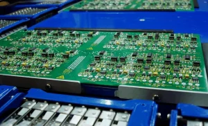
Fiducial marks should be surrounded by a clear area without solder mask or other features that could interfere with optical recognition.
A clearance area larger than the fiducial itself should be provided around each mark. As a general design guideline, maintaining approximately 1.5 mm or more of additional solder-mask clearance can help provide a reliable optical reference.
The final fiducial design should always follow the requirements of the SMT equipment and assembly manufacturer.
PCB Panelization and SMT Assembly
Panelization is closely related to automated SMT assembly. A well-designed panel allows multiple boards to move through solder paste printing, component placement, reflow soldering, inspection, and other manufacturing operations efficiently.
During panel design, engineers should consider the complete assembly process rather than only the PCB outline.
Important factors include:
- Panel dimensions
- Board-to-board spacing
- Tooling rails
- Fiducial marks
- Tooling holes
- Component edge clearance
- V-Cut or stamp-hole connections
- PCB thickness
- Board rigidity
- Depanelization requirements
GOPCBA provides integrated PCB Assembly solutions covering SMT, through-hole, mixed technology assembly, testing, and other manufacturing requirements.
How to Optimize PCB Panelization for Manufacturing
The best panel design is not necessarily the one that fits the maximum number of boards onto a sheet. A good panel must balance material utilization, assembly efficiency, mechanical stability, manufacturability, and final product requirements.
Before releasing the panel for production, engineers should verify:
- Whether the panel dimensions are compatible with production equipment.
- Whether the connection method matches the PCB outline.
- Whether components have sufficient edge clearance.
- Whether tooling edges are required.
- Whether fiducial marks are correctly positioned.
- Whether positioning holes are available.
- Whether large components interfere with fixtures.
- Whether V-Cut or stamp-hole separation will damage the PCB.
- Whether the panel provides sufficient mechanical strength.
- Whether the design has been reviewed for manufacturing and assembly requirements.
For complex projects, working directly with a PCB manufacturer during the panelization stage can help identify manufacturing risks before production begins.
PCB Panelization for Cost-Effective Production
Proper panelization can improve production efficiency while reducing unnecessary material waste and handling operations.
For small boards, panelization can increase the number of units processed during each manufacturing cycle. During SMT production, multiple boards can also be assembled simultaneously, reducing repeated machine loading and handling.
However, maximizing the number of boards per panel should not compromise manufacturability. Excessively tight spacing, insufficient tooling space, or poor connection design can increase production risks and create problems during depanelization.
Therefore, effective panelization should always balance PCB manufacturing efficiency with assembly reliability and final product requirements.
GOPCBA provides integrated PCB Manufacturing and assembly services, supporting projects from PCB fabrication through component assembly and testing.
Final Checklist for PCB Panelization
Before submitting panelized PCB files for manufacturing, use the following checklist:
- Confirm the panel dimensions.
- Confirm the number of PCB units per panel.
- Select the correct connection method.
- Verify V-Cut or stamp-hole locations.
- Check component-to-edge clearance.
- Add tooling edges when necessary.
- Add fiducial marks.
- Add positioning holes.
- Check clearance around tooling holes.
- Verify large-component locations.
- Confirm panel rigidity.
- Check compatibility with SMT equipment.
- Review depanelization requirements.
- Complete DFM and assembly checks before production.
A carefully engineered panel can improve manufacturing efficiency, simplify automated assembly, reduce material waste, and help maintain consistent production quality. By considering the panel structure, board connection method, tooling requirements, component clearance, and assembly process from the beginning, engineers can create a panel that is easier and more reliable to manufacture.