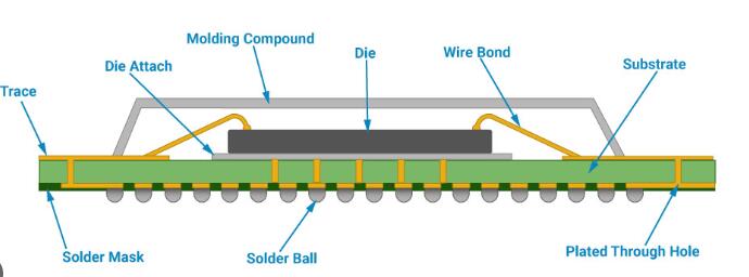
BGA Packaging, or Ball Grid Array packaging, is a surface-mount packaging technology widely used for integrated circuits (ICs) that require a high number of I/O connections within a compact package footprint. The development of BGA technology is closely related to the growing demand for electronic products that are smaller, lighter, more powerful, and more highly integrated.
As semiconductor devices continue to provide more functions and higher processing performance, conventional package designs can face limitations in I/O density and available connection space. Ball Grid Array technology addresses these challenges by arranging solder balls in an array on the underside of the package, allowing a large number of electrical connections to be accommodated within a relatively small area.
What Is BGA Packaging?
BGA Packaging is an IC packaging technology in which the electrical connections between the semiconductor package and PCB are formed by an array of solder balls on the bottom surface of the package.
Traditional surface-mount packages often use leads extending from the sides of the package. As the number of I/O connections increases, these leads can require more perimeter space and may limit package miniaturization.
By placing the solder connections underneath the package, Ball Grid Array technology makes more efficient use of the available package area. This structure can provide a higher I/O density while maintaining a compact footprint, making BGA particularly suitable for high-performance electronic products.
BGA packages are widely used in applications such as processors, memory devices, communication equipment, consumer electronics, networking products, automotive electronics, and industrial control systems.
Key Advantages of BGA Packaging
1. Efficient Use of PCB Space
One of the primary advantages of BGA Packaging is its ability to provide a high number of electrical connections without requiring a large package footprint.
Because the solder balls are arranged underneath the component rather than around its perimeter, more I/O connections can be accommodated within a limited area. This allows designers to make better use of PCB real estate and can contribute to overall product miniaturization.
For high-density PCB designs, BGA packages can also support more efficient component placement and routing compared with certain traditional leaded packages.
2. High I/O Density
BGA technology provides a practical solution for semiconductor devices with a large number of I/O connections.
Instead of extending leads outward from the package edges, the connections are distributed across the bottom surface. This two-dimensional arrangement allows the package to support a greater number of connections within a compact footprint.
As electronic devices become increasingly integrated, high I/O density has become an important factor in package selection.
3. Improved Electrical Performance
The relatively short electrical connection path between a BGA package and the PCB can help reduce parasitic inductance and capacitance compared with some longer-lead package structures.
This can be particularly beneficial for high-speed and high-frequency applications where signal integrity is strongly affected by interconnect characteristics.
However, actual electrical performance depends on the complete package and PCB design, including trace geometry, via structure, reference planes, material properties, power distribution, and signal routing.
Therefore, BGA Assembly should be considered together with PCB layout and signal-integrity requirements rather than evaluated solely by package type.
4. Good Thermal Performance
The large number of solder connections distributed beneath the package can provide multiple thermal and electrical paths between the component and PCB.
Depending on the package construction, PCB design, and thermal requirements, thermal vias and copper planes can be incorporated beneath the BGA area to help transfer heat away from the component.
For high-power devices, thermal management should be considered during both PCB design and PCB Assembly. The effectiveness of heat dissipation depends on factors such as copper area, via structure, board thickness, package design, and airflow.
5. Strong Mechanical Connection
BGA packages use solder joints distributed across the bottom of the component. The array structure provides numerous connection points between the package and PCB.
Unlike conventional packages with long external leads, there are no protruding leads that can easily be bent during handling. When the solder joints are properly formed and the assembly process is well controlled, BGA components can provide reliable mechanical and electrical connections.
Nevertheless, BGA solder joints remain sensitive to thermal-mechanical stresses. Board flexing, thermal cycling, solder-joint fatigue, and package-to-board coefficient of thermal expansion (CTE) mismatch should therefore be considered when evaluating long-term reliability.
BGA Soldering and Assembly Process
A critical part of BGA Assembly is ensuring that the solder balls form reliable connections between the component and PCB.
A typical BGA assembly process may include:
PCB Preparation → Solder Paste Printing → Component Placement → Reflow Soldering → Inspection → Electrical Testing
During solder paste printing, stencil design and printing parameters must be carefully controlled. Factors such as stencil thickness, aperture dimensions, paste volume, alignment, and printing consistency can directly affect solder-joint quality.
The BGA component is then accurately positioned on the PCB using a pick-and-place machine. During reflow, the solder paste melts and forms solder joints between the BGA balls and PCB pads.
Proper temperature-profile control is essential. Excessive heating, insufficient heating, or an inappropriate heating rate can result in defects such as insufficient soldering, solder bridging, voiding, or component warpage.
Challenges in BGA Assembly
Although BGA technology provides significant advantages, it also creates additional manufacturing and inspection challenges.
Because the solder joints are located beneath the component, they cannot normally be inspected effectively through conventional visual inspection after assembly.
This makes process control particularly important.
Common BGA-related defects may include:
- Solder bridging
- Insufficient solder
- Open solder joints
- Voids
- Head-in-pillow defects
- Component misalignment
- Solder ball deformation
- Non-wetting
- Pad contamination
- Warpage-related defects
Advanced inspection technologies such as X-ray inspection can be used to examine hidden solder joints and identify defects that are difficult to detect visually.
PCB Design Considerations for BGA Components
Successful BGA Assembly begins with appropriate PCB design.
When designing a PCB for a BGA component, engineers should consider:
- BGA pitch and ball diameter
- PCB pad dimensions
- Solder mask design
- Via diameter and aspect ratio
- Via-in-pad requirements
- Escape routing
- Layer count
- Controlled impedance
- Power and ground distribution
- Thermal management
- Manufacturing tolerances
For fine-pitch BGA components, conventional routing may not provide sufficient space to escape all signals from the inner rows. In such cases, designers may use techniques such as microvias, blind vias, stacked or staggered vias, and via-in-pad structures, depending on the PCB technology and manufacturing capability.
The selected design approach should always be evaluated against actual PCB Manufacturing capabilities to ensure that the board can be produced consistently.
BGA Solder Pad Design
BGA pad geometry has a direct influence on solder-joint formation.
Depending on the PCB process and component requirements, non-solder-mask-defined (NSMD) and solder-mask-defined (SMD) pad structures may be used.
The appropriate pad structure should be selected based on factors such as:
- BGA pitch
- Ball diameter
- PCB surface finish
- Solder mask capability
- Registration tolerance
- Assembly process
- Reliability requirements
For fine-pitch BGA devices, even small variations in pad dimensions or PCB registration can affect solder-joint quality. Therefore, close coordination between PCB design and manufacturing engineering is essential.
BGA Inspection and Quality Control
Because BGA solder joints are hidden beneath the component, inspection plays an important role in PCB Assembly quality control.
A comprehensive inspection strategy may include:
Solder Paste Inspection (SPI):
SPI verifies solder paste volume, position, and printing consistency before component placement.
Automated Optical Inspection (AOI):
AOI can inspect component placement and visible soldering characteristics, although it has limited visibility of hidden BGA joints.
X-Ray Inspection:
X-ray inspection is particularly valuable for BGA assemblies because it can examine hidden solder joints and identify defects such as voids, opens, shorts, and insufficient solder.
Electrical Testing:
Electrical testing can verify circuit connectivity and identify open or short circuits after assembly.
Using multiple inspection methods provides a more comprehensive approach to BGA quality control.
BGA Packaging and PCB Manufacturing
The introduction of BGA components places additional requirements on PCB Manufacturing.
As BGA pitch becomes smaller, the PCB may require:
- Finer line widths and spacing
- Higher registration accuracy
- Smaller vias
- Microvia technology
- More advanced multilayer structures
- Controlled impedance
- Improved solder mask registration
- Tighter manufacturing tolerances
Therefore, the PCB manufacturer must have the appropriate fabrication capabilities to support the selected BGA package.
For high-density applications, PCB fabrication and assembly should be considered as an integrated manufacturing process rather than as two completely independent stages.
BGA Reliability Considerations
BGA reliability depends on both package construction and assembly quality.
Thermal cycling can create mechanical stress because the PCB and semiconductor package typically have different CTE values. Repeated temperature changes can therefore place stress on solder joints over time.
Other factors that may affect BGA reliability include:
- PCB thickness and rigidity
- Component size
- Solder-joint geometry
- Reflow profile
- Board warpage
- Thermal cycling
- Mechanical vibration
- Drop and shock conditions
- Moisture exposure
- Assembly process consistency
For demanding applications, reliability testing and process validation should be performed according to the product’s operating environment and applicable industry requirements.
Kingda’s BGA PCB Manufacturing and Assembly Capabilities
At Kingda, BGA-related PCB production focuses on maintaining consistency across PCB fabrication, component assembly, and inspection.
For PCB designs incorporating high-density BGA packages, manufacturing considerations can be evaluated from the early design stage. Factors such as pad geometry, via structures, layer stackup, trace routing, registration accuracy, and assembly requirements can be coordinated to improve manufacturability.
During BGA Assembly, controlled solder paste printing, accurate component placement, optimized reflow profiles, and appropriate inspection methods help reduce assembly defects and improve production consistency.
By combining PCB fabrication expertise with systematic assembly and quality-control processes, Kingda supports BGA applications that require high density, reliable interconnection, and stable manufacturing performance.
Conclusion
BGA Packaging has become an important technology for modern electronic products that require high I/O density, compact dimensions, and reliable electrical performance.
By arranging solder balls beneath the package, Ball Grid Array technology makes efficient use of PCB space and provides a practical solution for highly integrated semiconductor devices. At the same time, BGA technology requires careful consideration of PCB layout, pad design, soldering, inspection, thermal management, and reliability.
A successful BGA Assembly process depends on close coordination between PCB design, PCB Manufacturing, and assembly engineering. With appropriate design rules, process control, inspection, and reliability management, BGA technology can provide a robust interconnection solution for advanced electronic products.