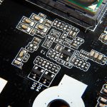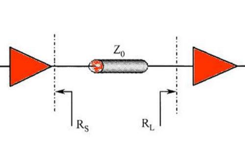
In high-speed PCB design, PCB impedance matching is an important technique for maintaining signal integrity and reducing signal reflections, overshoot, ringing, and electromagnetic interference. As signal rise times become faster and transmission distances increase, PCB traces can no longer always be treated as simple electrical connections. Instead, they may behave as transmission lines with characteristic impedance.
The basic principle of impedance matching is to make the impedance of the signal source, transmission line, and load compatible with each other. Depending on how the matching network is connected, impedance matching can generally be divided into series termination and parallel termination.
In practical PCB design, the appropriate termination method depends on signal frequency, rise time, trace length, source impedance, load characteristics, and interface standards.
Series Termination
Series termination is commonly used for high-speed digital signals and is particularly effective when a driver is connected to a relatively long PCB trace.
In embedded systems, when the signal frequency is above approximately 20 MHz and the PCB trace is longer than about 5 cm, designers may consider adding a series termination resistor. Typical applications include clock signals, data buses, address buses, and other fast digital signals.
The series resistor is normally placed close to the signal driver. Its resistance is selected according to the driver’s output impedance and the characteristic impedance of the PCB trace. Typical values may range from approximately 20 Ω to 75 Ω, although the actual value should be determined through signal-integrity analysis or measurement rather than by frequency alone.
The effectiveness of series termination is primarily related to signal rise time and transmission-line behavior. A signal with a very fast edge contains significant high-frequency components, even if its clock frequency itself is relatively low.
1. Reduce High-Frequency Noise and Overshoot
A fast signal edge contains many high-frequency components. When these components propagate along a PCB trace, they can increase electromagnetic radiation and make overshoot and ringing more likely.
A series resistor, together with the distributed capacitance of the PCB trace and the input capacitance of the receiving device, forms an effective RC network. This increases the rise and fall times of the signal and reduces the steepness of the edge.
As a result, series termination can help reduce high-frequency noise, overshoot, ringing, and unnecessary electromagnetic radiation.
However, the resistor should not be excessively large. Excessive resistance can slow the signal too much and may cause setup or timing violations.
2. Reduce High-Frequency Reflections and Ringing
When the electrical length of a PCB trace becomes significant compared with the signal’s rise-time-related propagation distance, the trace should be treated as a transmission line.
If the characteristic impedance of the transmission line does not match the effective impedance of the receiving or driving circuit, part of the signal energy is reflected.
These reflected signals can interfere with the original waveform, producing ringing, overshoot, undershoot, and other signal-integrity problems.
A properly selected series resistor increases the effective source impedance of the driver so that it more closely matches the characteristic impedance of the PCB transmission line.
For low-speed signals with short traces, transmission-line effects are usually negligible, and a series termination resistor may not be necessary.
Parallel Termination
Parallel termination, also known as shunt termination, is commonly used at the receiving end of a transmission line. It is particularly useful for high-speed interfaces where controlling signal reflections is important.
The termination resistor is connected between the signal line and a reference voltage or ground, depending on the interface and termination scheme.
For example, LVDS and RS-422/RS-485 interfaces using approximately 100 Ω differential transmission lines commonly require a 100 Ω termination resistor across the differential pair at the appropriate receiving end.
For video systems and other interfaces using coaxial cables, 50 Ω or 75 Ω termination may be used depending on the cable and system standard.
Unlike a series resistor, the value of a parallel termination resistor is primarily determined by the characteristic impedance of the transmission line and the electrical requirements of the interface.
Its main purpose is to absorb signal energy at the end of the transmission line and reduce reflections.
Series vs. Parallel Termination
The choice between series termination and parallel termination depends on the circuit topology and system requirements.
Series termination has several advantages:
- Simple circuit implementation
- Low DC power consumption
- Suitable for point-to-point digital signals
- Effective for controlling reflections near the signal source
- Helps reduce overshoot and ringing
Parallel termination offers different advantages:
- Strong control of signal reflections
- Suitable for certain high-speed buses and interface standards
- Effective at the receiving end of a transmission line
- Can provide a well-defined termination impedance
However, parallel termination may continuously consume power, depending on the termination topology. Therefore, power consumption must be considered in low-power systems.
Impedance Matching and EMI Performance
Proper PCB impedance matching does more than improve waveform quality. It can also contribute to better EMI performance.
Signal reflections and ringing can generate additional high-frequency energy that may couple into adjacent traces, planes, cables, or other circuit sections.
By controlling impedance discontinuities and reducing unnecessary reflections, designers can reduce unwanted high-frequency components and improve electromagnetic compatibility.
In addition to resistive termination, transformers can also be used for impedance conversion and isolation in certain interfaces. Common examples include Ethernet interfaces and some CAN bus applications.
Zero-Ohm Resistors in PCB Design
A zero-ohm resistor is not simply a resistor with literally zero resistance. It is a low-resistance component designed to function as a convenient link, configuration element, or debugging point in a PCB circuit.
Zero-ohm resistors are widely used in PCB design because they provide flexibility during development, manufacturing, testing, and maintenance.
1. Function as a Jumper
A zero-ohm resistor can be used as a PCB jumper to connect two circuit sections without using a separate wire.
This approach provides a cleaner and more automated manufacturing solution than manually soldering jumper wires.
If the connection is not required in a particular product configuration, the zero-ohm resistor can simply be omitted during assembly.
2. Simplify Circuit Debugging
When the exact value of a matching resistor is uncertain during the initial design stage, a zero-ohm resistor can temporarily be installed.
During prototype testing, engineers can replace it with a resistor of the appropriate value after measuring the actual signal waveform.
This provides a convenient way to optimize impedance matching without redesigning the PCB.
3. Facilitate Current Measurement
A zero-ohm resistor can also serve as a convenient current-measurement point.
During testing, the resistor can be removed and replaced temporarily with an ammeter or current-measuring instrument. This allows engineers to measure the current flowing through a particular circuit branch.
For production designs, however, the measurement method and resulting contact resistance should be considered carefully.
4. Isolate Power and Ground Sections
Zero-ohm resistors can be used to separate different circuit sections during debugging.
For example, a system may contain several functional modules with independent power or ground connections. Installing a zero-ohm resistor between these sections makes it possible to isolate individual modules during troubleshooting.
If a short circuit occurs, removing the corresponding zero-ohm resistor can help narrow down the location of the fault.
This technique is especially useful during prototype development and board-level troubleshooting.
5. Configure Different PCB Versions
A zero-ohm resistor can also be used as a configuration option.
By installing or omitting specific zero-ohm resistors, manufacturers can create different hardware configurations from the same PCB layout.
This can reduce the need to develop multiple PCB versions for products with different functional requirements.
Zero-Ohm Resistors in High-Speed Signal Networks
Although a zero-ohm resistor is primarily used as a jumper or configuration component, its physical package and PCB footprint still introduce parasitic resistance and inductance.
At high frequencies, these parasitic effects can influence signal integrity.
Therefore, a zero-ohm resistor should not automatically be considered electrically identical to a copper trace, especially in very high-speed applications.
In some circuits, a resistor footprint can also provide a convenient location for future signal-integrity optimization. During prototype testing, the zero-ohm resistor can be replaced by a specific series resistance if measurements show that series termination is required.
This approach allows designers to maintain flexibility without changing the PCB layout.
Single-Point Grounding
Zero-ohm resistors may also be used to implement controlled connections between different ground domains.
For example, analog and digital ground sections may be connected at a carefully selected single point to control return-current paths and reduce unwanted coupling.
However, the use of a zero-ohm resistor for grounding should be based on the actual current-return architecture and system EMC requirements. Simply separating analog and digital ground with a resistor does not automatically improve EMI performance.
A well-designed ground plane and controlled return path are often more important than the component itself.
Practical PCB Impedance Matching Guidelines
When implementing PCB impedance matching, designers should consider the following factors:
- Evaluate signal rise time, not only the nominal clock frequency.
- Control PCB trace impedance through appropriate trace width, dielectric thickness, copper thickness, and stack-up design.
- Place series termination resistors close to the signal driver whenever possible.
- Place parallel termination at the appropriate receiving end according to the interface topology.
- Minimize unnecessary vias and impedance discontinuities in high-speed signal paths.
- Maintain a continuous reference plane beneath high-speed traces.
- Keep differential-pair geometry consistent and control differential impedance.
- Use simulation or oscilloscope measurements to determine the actual termination value when necessary.
- Consider power consumption when using parallel termination.
- Use zero-ohm resistors strategically for configuration, debugging, isolation, and future optimization.
Conclusion
As PCB operating speeds continue to increase, PCB impedance matching becomes increasingly important for maintaining reliable signal transmission.
Series termination is a practical solution for controlling reflections and slowing excessively fast signal edges, while parallel termination can effectively absorb reflected energy at the receiving end of a transmission line.
At the same time, zero-ohm resistors provide valuable flexibility during PCB development, debugging, configuration, and manufacturing.
For complex high-speed PCB designs, impedance matching should be considered together with PCB stack-up, trace geometry, reference planes, component placement, return-current paths, and signal integrity requirements.
Kingda can support PCB design and manufacturing requirements where controlled impedance, high-speed signal routing, and reliable PCB assembly are essential. By combining appropriate PCB materials, controlled manufacturing processes, and impedance-aware design practices, engineers can build more stable and reliable electronic systems.