
How Strict Testing Ensures Long High-Speed PCB Life
A high-speed high-frequency board can pass every visual check and still fail in the field. The failure often starts long before shipment, in a material batch, a lamination cycle, or a surface finish that drifted. Strict testing exists to catch those drifts while they are still cheap to correct. This article walks through the four test stages that protect board life, from incoming material to application compatibility. Each stage answers a different question, and each one feeds the next.
Lifespan is not a single property that can be measured once. It is the combined result of material stability, process control, finished performance, and fit with the operating environment. A board that survives one test may still degrade under another stress. Buyers and engineers therefore need a test plan that covers all four areas and records the results. Without records, a good batch proves nothing about the next one. The sections below explain what each test looks for and what to verify.
Material Verification First
The substrate, copper foil, and solder mask set the ceiling on reliability. If a raw material carries a hidden weakness, no amount of process control will fully compensate. Incoming inspection should therefore begin before production, not after. Material testing identifies problems at the point where replacement is still simple. A supplier that skips this step is trusting the certificate alone, and certificates describe the batch, not the board.
Environmental aging tests expose substrate samples to cyclic temperature and humidity. After a defined period, key parameters such as dielectric constant, dissipation factor, and mechanical strength are measured again. Stable values indicate good aging resistance. Large shifts suggest that a more durable material should be selected. For high-frequency work, the dielectric parameters matter most, because small changes alter impedance and loss. The test period and limits should be agreed in writing before the lot starts.
Copper adhesion decides whether traces stay attached through vibration and thermal cycling. Peel testing measures the bond between foil and substrate. Samples can also run through repeated environmental cycles before the peel test, which shows whether the bond holds after exposure. Weak adhesion may open a circuit only after months of service, when the cause is hard to find. Recording peel results per lot gives the buyer a trend to review. A falling trend is an early warning, even when every value still passes.
The solder mask protects copper from contamination and chemical attack. Poor chemical resistance shows up as discoloration, blistering, cracking, or peeling. Once the mask breaks down, exposed circuitry corrodes faster. Testing exposes coated samples to chemicals representative of the intended environment, then checks the surface and the electrical behavior. The mask must keep insulating after exposure, not just look intact. Buyers should confirm which chemicals were used, because a generic test may not match the real application.
Process Reliability Checks
Good materials cannot rescue a weak process. Insufficient lamination, etching residue, and uneven surface finish all create hidden risks that appear later as field failures. Process testing targets these risks directly, at the stage where they are created. It also connects to quality management, because every process check produces data that must be reviewed and acted on. A check that is recorded but never reviewed adds cost without adding protection. The goal is a closed loop between measurement and correction.
Lamination turns stacked layers into one structure. If interlayer bonding is weak, thermal cycling and mechanical stress may eventually cause delamination. Bonding-strength tests on laminated samples verify that adhesion meets the agreed criteria. Samples can also be held at elevated temperature, then inspected for bubbles or separation. These tests confirm that the press profile suits the material set. Any change in prepreg, press cycle, or panel design should trigger a fresh check, because lamination behavior is sensitive to all three.
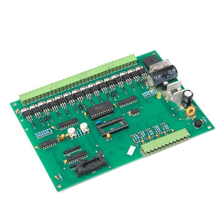
Etching defects include burrs, residual copper, and irregular trace edges. High-magnification inspection finds these irregularities before they become electrical or thermal stress points. Long-term electrical testing can then reveal abnormal temperature rise near a suspect trace. Precise etch control reduces the risk at the source, and inspection confirms the control worked. The two belong together. A buyer reviewing a supplier should ask how trace edges are inspected and how often the etchant is analyzed. Frequent analysis is a sign that the process is managed, not just run.
Surface finishes such as ENIG and OSP protect against oxidation and support solderability. Uneven thickness creates weak spots that oxidize first. Insufficient wear resistance causes damage during assembly, insertion, or repeated contact. Testing measures thickness distribution and applies simulated friction or insertion cycles. The finish must keep protecting the copper through the intended service period, not merely at incoming inspection. Buyers should match the finish to the assembly process and the contact duty, then confirm the supplier tests what was specified.
Finished Board Verification
Once materials and processes are validated, the finished board faces its own tests. A board can remain physically intact while its electrical performance slowly declines. Finished-product testing looks for that decline under extended operation. Samples connect to a simulated system and run for a defined period, with parameters monitored at intervals. Stable signal loss and interference indicate good long-term transmission. Degradation sends the investigation back to materials and processes. This stage is where rapid PCBA prototyping helps, because early samples can be tested before volume is committed.
Mechanical fatigue is a common cause of late failure. Boards inside equipment see continuous vibration and repeated stress. Over time, traces can crack and substrates can damage. Fatigue testing applies periodic stress to finished samples, then inspects for structural damage and rechecks electrical performance. The combined view matters, because a board may look sound while its resistance has risen. The number of cycles and the inspection criteria should reflect the real mounting and handling. Buyers should ask whether the test fixture resembles the actual installation.
Conductivity can fall over time through oxidation, poor contact, or process defects. Critical circuits can be loaded continuously while resistance is monitored at regular intervals. Stable resistance shows the conductive path remains sound. A clear rise points to oxidation, contact problems, or a manufacturing defect, and it should trigger investigation rather than acceptance. This test is simple and informative, which makes it a practical addition to most programs. It also gives the buyer a numeric record to compare across lots and suppliers.
Application Compatibility
Laboratory performance does not guarantee field performance. Each product exposes the board to its own temperatures, stresses, and nearby components. Compatibility testing checks the board inside conditions that resemble the final system. Thermal testing installs the board in the target equipment and runs it under simulated load. Temperature distribution across critical areas is then monitored. Acceptable temperatures indicate good thermal fit. Local hot spots suggest that board position, thermal design, or the cooling solution needs work. Catching this before launch avoids a costly redesign.
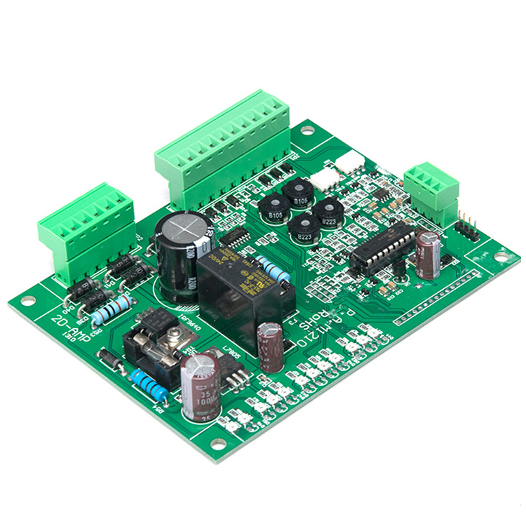
Boards also share space with ICs, connectors, power devices, and modules. Poor compatibility raises interference, distorts current distribution, and creates local heating. Over time, these effects age both the board and its neighbors. Testing should therefore evaluate the board together with the major components in a simulated environment. Signal integrity, current distribution, and temperature are monitored together. A system that runs normally under this combined test is far more likely to survive real service. Buyers should confirm that the test setup includes the components that generate heat and noise.
Building the Test Loop
A single final inspection cannot protect lifespan. A complete loop covers materials, processes, finished boards, and application conditions. Material testing finds weaknesses in substrates, foil, and mask. Process testing finds delamination, trace irregularities, and finish problems. Finished testing measures long-term electrical and mechanical behavior. Application testing confirms the board works in its real thermal, electrical, and mechanical setting. Each stage catches what the others miss, and each stage depends on the records the previous one produced.
This layered approach finds problems as early as possible, before the board reaches a customer. It also supports PCB design and layout reviews, because test results often reveal design choices that stress the process. When a test fails, the response should trace back to the cause, not just screen out the failed unit. Suppliers that treat test data as feedback improve over time. Suppliers that treat it as paperwork repeat the same defects. Buyers can tell the difference by asking what changed after the last failure.
What Buyers Should Verify
Test methods and acceptance limits should match the board structure, materials, environment, and end use. A generic plan copied from another product proves little. Ask which tests run on every lot and which run only at qualification. Ask how samples are selected and how failures are handled. Ask for the records, not just the pass statement. A supplier that can produce clear records on request usually keeps them honestly during production. That habit is the real foundation of long board life.
Documentation should travel with the lot. The record should show which program ran, which materials were used, and what inspection found. When a field return arrives months later, that record is the fastest route to the cause. It also proves that a fix reached the next batch. Buyers should make these records a routine part of every order, alongside component procurement checks that confirm what went onto the board. Traceability connects the test result to the exact build.
For programs moving into volume, the test plan must scale without losing coverage. Sampling rates, fixture capacity, and data handling all need review as quantities grow. High-volume PCB assembly places more demand on test throughput, and a plan that worked for prototypes may become a bottleneck. The fix is to automate data collection and keep the critical tests intact. Buyers should confirm that coverage does not shrink as volume rises. A test plan that quietly weakens under schedule pressure is worse than no plan, because it hides risk.
The practical takeaway is simple. Ask for a written test plan that names each stage, the sample size, the acceptance limit, and the record kept. Compare that plan with the application, then check whether the last three lots followed it. Strict testing protects board life only when it is specific, recorded, and reviewed. Everything else is inspection theater. Engineers and buyers who insist on those four elements get boards that behave predictably in the field, and they learn about problems while the fix is still inexpensive.