Any-Layer Interconnect PCB: A Professional Solution for High-Density Electronics
As electronic devices continue to become smaller, faster, and more functionally integrated, conventional PCB interconnection structures are facing increasing design challenges. Traditional layer-to-layer interconnection can limit routing flexibility, consume valuable board space, and create additional signal paths.
An Any-Layer Interconnect PCB provides a more flexible approach to high-density circuit design. By enabling connections between different circuit layers through advanced microvia and sequential build-up technologies, this PCB architecture can support compact layouts, shorter signal paths, and higher routing density.
These characteristics make any-layer interconnect technology particularly valuable for telecommunications, automotive electronics, medical equipment, computing systems, and other demanding applications.
1. Core Technology Features of Any-Layer Interconnect PCB
The primary advantage of an Any-Layer Interconnect PCB is its ability to overcome the limitations of conventional layer-to-layer interconnection.
Instead of relying exclusively on fixed through-hole structures to connect specific layers, any-layer technology uses advanced microvia structures and build-up processes to create more flexible electrical connections between circuit layers.
1.1 Laser Microvia Technology
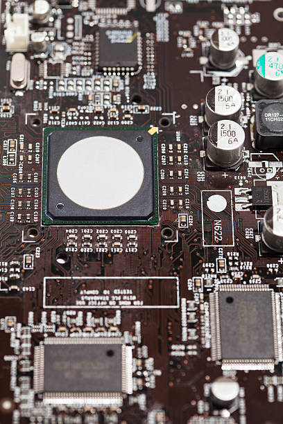
Laser drilling is one of the key technologies behind any-layer interconnection.
High-precision laser equipment creates very small microvias in the PCB dielectric material. These microvias can establish electrical connections between adjacent build-up layers while minimizing the space required for conventional vias.
Compared with larger mechanical vias, microvias can provide greater routing flexibility and help reduce unnecessary signal-path transitions.
This makes laser drilling particularly important for applications requiring fine-pitch components and dense routing, which are common characteristics of modern HDI PCB designs.
1.2 Sequential Build-Up Technology
Sequential build-up technology creates the PCB structure by repeatedly adding dielectric and conductive layers.
Each build-up cycle can incorporate processes such as lamination, laser drilling, copper plating, and circuit formation. This allows designers to develop a three-dimensional interconnection structure in which different circuit layers can be connected according to routing requirements.
Rather than being constrained by a single fixed interconnection structure, designers gain greater freedom to optimize the location and direction of signal paths.
1.3 High-Density Routing Capability
Flexible interconnection also improves PCB space utilization.
Because routing does not need to accommodate as many conventional through-hole structures, more circuit traces and component connections can be placed within a given board area.
This is particularly useful for compact electronic products where board size is tightly constrained but circuit functionality continues to increase.
For projects requiring advanced board fabrication capabilities, GOPCBA provides comprehensive PCB Manufacturing Services covering complex multilayer structures and high-density PCB requirements.
2. Key Advantages of Any-Layer Interconnect PCB
2.1 Improved Signal Transmission Performance
Signal integrity is critical in high-frequency and high-speed electronic systems.
An Any-Layer Interconnect PCB can shorten signal transmission paths and reduce unnecessary vias and routing transitions. This can help minimize signal delay, discontinuities, and potential crosstalk.
For example, in a 5G communication system, shorter and more direct routing paths can help improve the electrical environment for high-speed RF and digital signals.
For demanding applications, the overall board design must also consider controlled impedance, material selection, stack-up design, and manufacturing tolerances. The PCB structure and manufacturing process should therefore be developed together rather than treated as separate engineering tasks.
2.2 Better Utilization of Board Space
Miniaturization is one of the most important requirements in modern electronic product development.
Wearable devices, smartphones, portable medical equipment, and other compact products need to accommodate increasing numbers of components and interfaces without significantly increasing their physical dimensions.
The three-dimensional interconnection structure of any-layer PCB allows routing resources to be distributed more efficiently throughout the board.
As a result, manufacturers can potentially achieve thinner and more compact PCB designs while maintaining the required circuit functionality.
This makes the technology particularly suitable for High-Density PCB applications where routing space is limited.
2.3 Enhanced Structural Reliability
Reliability is another important consideration for advanced multilayer PCB structures.
Laser-formed microvias with appropriate copper plating can provide reliable electrical connections between build-up layers. Properly controlled dielectric and conductive layer bonding can also help the PCB withstand thermal cycling, mechanical vibration, and other environmental stresses.
However, reliability depends heavily on material selection, via structure, copper plating quality, lamination parameters, and process control.
For this reason, advanced PCB Manufacturing should include appropriate engineering review, process validation, and inspection throughout production rather than relying only on final inspection.
3. Industry Applications of Any-Layer Interconnect PCB
3.1 Automotive Electronics
The rapid development of electric vehicles, advanced driver-assistance systems, and autonomous driving is increasing the demand for compact, high-performance automotive electronics.
Modern vehicles may incorporate radar sensors, cameras, LiDAR systems, domain controllers, communication modules, and other electronic systems that require high-density signal routing.
An any-layer PCB can provide flexible interconnections for these systems while helping designers manage limited board space.
In high-temperature or mechanically demanding automotive environments, the PCB must also be designed and manufactured with appropriate materials, thermal characteristics, mechanical reliability, and process controls.
3.2 Medical Equipment
Medical electronics often require high circuit density while maintaining stable electrical performance and compact product dimensions.
Portable ultrasound equipment, imaging systems, patient monitoring devices, and other sophisticated medical products may integrate multiple signal acquisition, processing, and communication functions into a relatively small space.
An any-layer interconnection structure can provide additional routing flexibility for these complex circuits.
For projects that require both PCB fabrication and electronic assembly, GOPCBA also offers Prototype PCB Assembly to support early-stage product validation before production scaling.
3.3 Telecommunications and Data Infrastructure
5G base stations, networking equipment, high-speed switches, and data-processing systems place demanding requirements on PCB signal transmission.
These systems may contain high-speed interfaces and multiple communication channels that require careful routing and impedance control.
Any-layer interconnect technology can help designers optimize high-speed signal paths and increase routing density within complex multilayer boards.
When combined with appropriate low-loss materials and controlled manufacturing processes, the structure can support demanding High-Speed PCB applications.
4. Any-Layer Interconnect PCB Development Trends
As artificial intelligence, high-performance computing, IoT, advanced communications, and other technologies continue to evolve, PCB designs are moving toward higher density, faster signal transmission, and greater miniaturization.
Any-layer interconnect technology is expected to continue developing in several key areas.
4.1 Smaller Microvia Structures
As component packaging becomes increasingly compact, PCB manufacturers will need to support smaller and more precisely controlled microvia structures.
Advances in laser drilling and related inspection technologies can help accommodate finer-pitch components and increasingly dense circuit layouts.
4.2 Advanced Low-Loss Materials
Material technology will also play an increasingly important role.
For high-speed applications, lower-loss and lower-dielectric-constant materials can help reduce transmission losses and improve electrical performance.
Material selection must be matched to the operating frequency, stack-up configuration, impedance requirements, thermal conditions, and manufacturing process.
4.3 Manufacturing Cost Optimization
One of the challenges of any-layer PCB technology is the complexity of its manufacturing process.
Laser drilling, sequential lamination, microvia formation, copper plating, and inspection all require precise process control and specialized equipment.
As production equipment becomes more automated and manufacturing processes become more mature, production efficiency can improve and manufacturing costs may become more competitive.
This could expand any-layer interconnect technology into a broader range of electronic products beyond the most advanced applications.
5. How to Build a Reliable Any-Layer PCB Solution
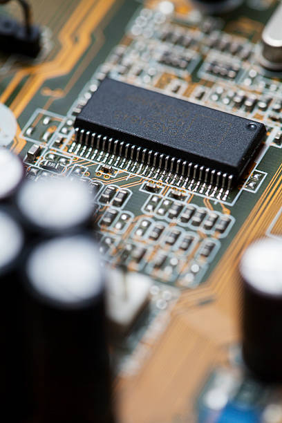
A successful any-layer PCB project requires more than simply selecting a high-density board structure.
The design and manufacturing process should be considered as an integrated engineering workflow.
Key considerations include:
- Stack-up design: Define appropriate dielectric thicknesses, copper weights, and signal/reference-layer relationships.
- Microvia design: Select suitable via dimensions and structures according to component pitch and routing density.
- Material selection: Match PCB materials to frequency, thermal, mechanical, and reliability requirements.
- Signal integrity: Control impedance and minimize unnecessary discontinuities in high-speed signal paths.
- Manufacturing feasibility: Confirm that the proposed structure can be produced consistently within the required tolerances.
- Testing and inspection: Establish appropriate electrical, dimensional, and structural inspection procedures.
For customers requiring a complete production solution, GOPCBA can also combine PCB fabrication with assembly and component sourcing through its Turnkey PCB Assembly Services.
6. The Role of Any-Layer Technology in Future Electronics
Any-layer interconnect technology represents an important development direction for advanced PCB design.
By combining laser microvias, sequential build-up structures, high-density routing, and advanced materials, it provides designers with greater freedom to integrate complex circuits into smaller form factors.
Its value is particularly evident in applications where high-speed performance, compact dimensions, routing density, and reliability must be achieved simultaneously.
As electronic systems continue to evolve, the demand for advanced HDI PCB, High-Density PCB, and High-Speed PCB solutions is expected to grow.
At the same time, successful implementation will depend on close coordination between PCB design, material selection, fabrication, assembly, testing, and quality management.
Conclusion
The Any-Layer Interconnect PCB provides a flexible and highly integrated approach to solving the routing and space limitations of conventional PCB structures.
Through laser microvia technology and sequential build-up processes, it can increase routing density, shorten signal paths, improve space utilization, and support compact high-performance electronic products.
From automotive electronics and medical equipment to 5G communications and high-speed computing, any-layer interconnection technology can provide an effective foundation for increasingly complex electronic systems.
As PCB technology continues to advance, improvements in microvia fabrication, low-loss materials, automation, and process control will further enhance the practicality and cost competitiveness of any-layer PCB solutions.