Low-Power PCB for IoT Devices: Key Design and Manufacturing Considerations
Low-Power PCB for IoT Devices
The rapid growth of the Internet of Things (IoT) has led to the widespread deployment of connected devices in smart homes, industrial monitoring, environmental sensing, healthcare, and other applications. Many of these devices are expected to operate continuously for long periods while consuming very little energy.
At the heart of these systems is the low-power PCB, which provides the electrical connections and physical platform required to integrate sensors, processors, wireless communication modules, power circuits, and other components.
For battery-powered or energy-constrained IoT products, PCB design is not simply about connecting components. It also involves optimizing power distribution, signal integrity, thermal behavior, electromagnetic compatibility, and component placement to support reliable long-term operation.
1. Efficient Energy Management
One of the most important functions of a low-power PCB is to support efficient energy distribution throughout the IoT device.
Many IoT terminals operate from batteries or limited energy sources. Some remote monitoring devices may need to operate for months or even years without frequent maintenance. In these applications, unnecessary power consumption can directly reduce operating time.
A well-designed PCB can help divide the system into different power domains. Non-essential circuits can be switched off or placed into low-power states when the device enters sleep mode, while essential functions such as sensing, timing, or wireless communication remain active.
When the device needs to perform a measurement or transmit data, the corresponding circuits can be activated according to the system’s power-control strategy.
This makes PCB power management an important part of IoT hardware design. Engineers should consider power paths, voltage regulation, grounding, decoupling, component selection, and standby-current requirements during the PCB design stage.
For projects requiring professional circuit planning and manufacturability analysis, PCB Design & Layout can help establish an appropriate foundation before fabrication.
2. Environmental Adaptability and EMI Protection
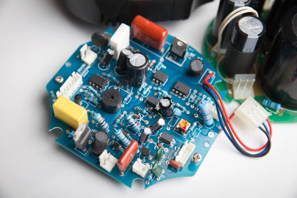
IoT devices are often installed in environments that are very different from those of conventional consumer electronics.
Depending on the application, an IoT terminal may be deployed in:
- Industrial workshops
- Outdoor monitoring stations
- Agricultural environments
- Smart buildings
- Transportation systems
- Remote infrastructure
- Dusty or humid locations
These environments can expose PCBs to temperature fluctuations, humidity, vibration, dust, and electromagnetic interference.
PCB material selection, surface finishing, component selection, grounding, shielding, and layout design can all influence the reliability of the finished board.
For example, sensitive communication and sensor circuits should be carefully separated from noisy power-switching sections when required by the design. Appropriate ground structures and decoupling networks can also help reduce unwanted interference.
For applications with more demanding electrical requirements, material selection and controlled fabrication parameters should be evaluated together rather than treating the PCB as an isolated mechanical component.
3. Flexible Layout for Different IoT Functions
IoT devices can vary considerably in functionality and physical size. A simple temperature sensor may require only a microcontroller, sensor, power circuit, and wireless module, while an industrial monitoring terminal may integrate multiple sensors, processing units, communication interfaces, memory, and power-management circuits.
This makes layout flexibility another important characteristic of an IoT PCB.
PCB designers need to consider the relationship between:
- Sensors and processing devices
- Wireless communication modules
- Power-management circuits
- Antenna areas
- High-speed interfaces
- Connectors
- Mechanical mounting points
- Thermal-sensitive components
For wireless IoT products, antenna placement and RF routing deserve particular attention. Unnecessary trace length, inappropriate grounding, or interference from nearby switching circuits can affect wireless performance.
At the same time, compact IoT products may require multilayer PCB structures to provide sufficient routing space while maintaining a small form factor.
4. PCB Materials and Manufacturing Considerations
The material selected for an IoT PCB should match the electrical, mechanical, thermal, and environmental requirements of the final product.
For many conventional IoT applications, FR-4 remains a practical choice because of its balance of electrical performance, mechanical strength, availability, and cost. However, applications involving high-frequency wireless communication, demanding signal integrity, or specialized environmental requirements may require alternative or hybrid material solutions.
The manufacturing process is equally important. Factors such as trace geometry, via structures, layer alignment, copper thickness, solder mask, surface finish, and board flatness can influence the performance and reliability of the finished PCB.
Professional PCB manufacturing should therefore consider both the original electrical design and the practical requirements of volume production.
GOPCBA supports PCB fabrication from prototypes through production, providing a manufacturing path for projects with different complexity and volume requirements. PCB Manufacturing
5. PCB Assembly for IoT Devices
PCB fabrication is only one stage of the overall hardware production process. After the bare board is manufactured, components must be accurately placed, soldered, inspected, and tested.
IoT products often contain small packages, fine-pitch components, wireless modules, sensors, and power-management ICs. These components require appropriate assembly processes and inspection methods.
Depending on the product structure, manufacturers may use:
- SMT assembly
- Through-hole assembly
- Mixed-technology assembly
- Automated optical inspection
- X-ray inspection where appropriate
- Electrical testing
- Functional testing
Reliable PCB assembly helps ensure that the electrical design is correctly translated into a working product.
For early-stage IoT development, prototype assembly is particularly useful because it allows engineers to verify component placement, electrical functionality, mechanical compatibility, and manufacturing feasibility before committing to larger production quantities.
For this stage, Prototype PCB Assembly provides a practical route from PCB design verification to production preparation.
6. Designing for Long Battery Life
Low power consumption should be considered throughout the entire hardware design rather than added as an afterthought.
Several factors can influence the energy consumption of an IoT device:
Component Selection
Low-power microcontrollers, sensors, memory devices, communication modules, and voltage regulators can reduce overall system consumption when appropriately selected.
Sleep and Wake-Up Modes
Many IoT systems spend most of their operating time in standby or sleep mode. PCB and circuit design should support efficient transitions between active and low-power states.
Power Distribution
Short and appropriately designed power paths can help reduce unnecessary losses. Decoupling capacitors should also be positioned appropriately relative to sensitive ICs.
Wireless Communication
Wireless transmission can consume significantly more energy than many sensing operations. Optimizing transmission frequency, packet size, communication protocols, and RF circuit design can therefore have a substantial effect on battery life.
Thermal Management
Although many IoT devices operate at relatively low power, high-density designs or power-intensive communication circuits can still generate localized heat. Appropriate component placement and copper structures can help manage thermal conditions.
7. From Prototype to Low-Volume Production
IoT hardware development typically involves several stages, from concept and prototype validation to pilot production and eventual mass manufacturing.
At the prototype stage, engineers can identify issues such as:
- Incorrect component footprints
- Routing problems
- Power distribution issues
- RF interference
- Mechanical conflicts
- Assembly difficulties
- Unexpected thermal behavior
After the design has been validated, low-volume production can be used to evaluate manufacturing consistency and real-world product performance before larger-scale production.
GOPCBA also provides Low Volume PCB Assembly for projects that need to move beyond prototypes while maintaining production flexibility.
8. Future Development of Low-Power IoT PCBs
As IoT applications continue to expand, PCB technology will need to support increasingly smaller, smarter, and more energy-efficient devices.
Several developments are likely to remain important:
- More efficient power-management architectures
- Smaller and higher-density PCB designs
- Improved RF and high-frequency performance
- Advanced embedded sensing technologies
- Energy harvesting from solar, vibration, or other sources
- Better thermal and environmental reliability
- Greater integration of processing, communication, and sensing functions
Energy harvesting is particularly interesting for remote IoT applications. Solar cells, vibration-based systems, and other energy sources can potentially supplement or replace conventional batteries in specific applications. The PCB must then accommodate power-conditioning and energy-storage circuits suitable for the selected energy source.
Conclusion
A reliable low-power PCB is an important foundation for long-lasting IoT devices. Its role extends beyond basic electrical interconnection to include efficient energy distribution, signal integrity, environmental adaptability, electromagnetic compatibility, compact layout, and manufacturing reliability.
For an IoT PCB, the best results come from considering circuit design, material selection, PCB power management, fabrication, and assembly as one integrated development process.
By combining appropriate design practices with controlled PCB manufacturing and reliable PCB assembly, developers can create IoT hardware that is better suited to long-term operation, compact product designs, and increasingly demanding connected-device applications.