EV charging station PCB Power Module PCB: Design and Manufacturing Requirements
EV Charging Station Power Module PCB: A Critical Part of Charging Infrastructure
The rapid expansion of electric vehicles (EVs) is driving strong demand for reliable and efficient charging infrastructure. Whether used in residential garages, commercial parking facilities, or high-power public charging stations, charging equipment must safely convert and deliver electrical energy to the vehicle battery.
A critical part of this system is the power module PCB.
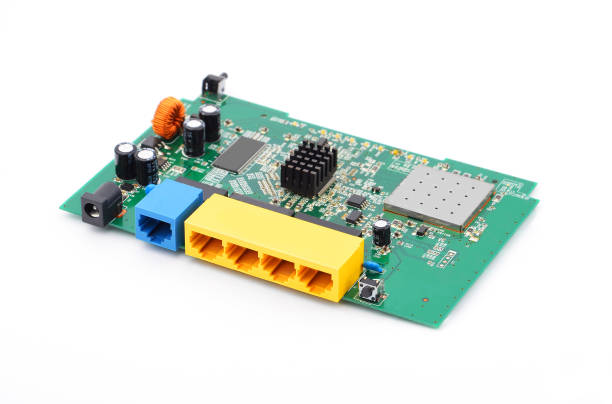
The PCB inside a charging power module provides electrical interconnections between power-conversion devices, control circuits, sensors, protection components, and communication interfaces. Its design can directly influence current distribution, thermal performance, signal integrity, and overall system reliability.
For high-power charging applications, PCB design and manufacturing must be carefully coordinated to handle substantial electrical loads while maintaining appropriate thermal and mechanical performance.
1. High-Current Power Transmission
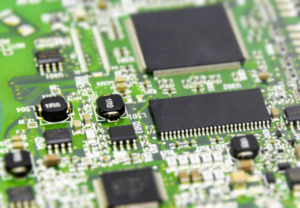
The primary role of an EV charging station PCB within a power module is to provide reliable electrical interconnection between critical power-conversion components.
During charging, electrical energy from the grid may pass through several conversion stages, including rectification, power-factor correction, DC conversion, and other power-processing functions before being delivered to the vehicle battery.
The PCB must therefore be designed around the expected current, voltage, temperature rise, and mechanical constraints.
Important design considerations can include:
- Copper thickness
- Trace width
- Current density
- Power-plane structure
- Via configuration
- Thermal dissipation
- Clearance and creepage requirements
- Connection between power and control circuits
For high-current paths, appropriately sized copper structures can help reduce electrical resistance and associated heat generation. However, copper thickness should be selected according to the complete electrical and manufacturing requirements rather than simply maximizing copper weight.
A carefully engineered layout can also help distribute current more evenly and reduce localized thermal stress.
2. Thermal Management for High-Power Charging
Thermal management is one of the most important considerations for a power module PCB.
High-power charging systems can generate substantial heat in switching devices, rectifiers, transformers, inductors, connectors, and other components. If heat is not effectively managed, excessive temperature can affect component performance and long-term reliability.
PCB design can contribute to thermal management through:
Copper Distribution
Larger copper areas can provide additional thermal conduction paths and may help spread heat away from high-power components.
Thermal Vias
Thermal vias can transfer heat between PCB layers or toward an appropriate heat-dissipation structure when the board construction supports this approach.
Component Placement
Power components should be positioned with consideration for heat sources, airflow, heatsinks, and temperature-sensitive devices.
Material Selection
Depending on the application, standard FR-4, high-Tg materials, heavy-copper constructions, or other specialized PCB technologies may be considered.
For demanding power electronics applications, material selection and board construction should be evaluated together with the thermal design.
3. Reliability in Outdoor Charging Environments
Unlike many indoor electronic products, EV charging stations are commonly installed in outdoor or semi-outdoor environments.
An EV charging station PCB may be exposed to:
- Temperature fluctuations
- High humidity
- Dust and contaminants
- Vibration
- Electrical transients
- Electromagnetic interference
- Repeated heating and cooling cycles
These conditions make environmental reliability an important part of PCB development.
The appropriate PCB material, surface finish, solder mask, component selection, enclosure design, and manufacturing process should be selected according to the operating environment.
For example, moisture and contamination can contribute to insulation degradation or corrosion under unsuitable conditions. Appropriate design clearances, surface protection, and material selection can help reduce these risks.
Electrical design should also consider electromagnetic compatibility. Separating noisy switching circuits from sensitive control or communication circuits, using suitable grounding strategies, and optimizing return-current paths can help improve system-level EMC performance.
4. Flexible Architecture for Different Charging Power Levels
Charging equipment is available in many different configurations, ranging from relatively low-power residential systems to high-power commercial and public fast-charging platforms.
These products can differ significantly in:
- Input voltage
- Output voltage
- Output current
- Charging power
- Cooling method
- Power-conversion topology
- Communication interfaces
- Physical dimensions
Consequently, PCB architecture needs to match the requirements of the particular charging platform.
A residential charger may prioritize compact dimensions and cost efficiency, while a high-power charging system may require heavier copper, more robust thermal structures, larger clearances, and additional sensing and protection circuitry.
The PCB should therefore be designed around the electrical and mechanical requirements of the intended power module instead of applying a single configuration to every charging application.
5. PCB Power Management and Control Circuits
Although power transmission is a major function of a charging power module, control and monitoring circuits are equally important.
Modern charging systems typically need to monitor parameters such as:
- Voltage
- Current
- Temperature
- Fault conditions
- Charging status
- Protection states
- Communication signals
The control circuitry must interact reliably with the power stage while maintaining appropriate isolation and noise control where required.
This makes PCB power management closely connected to both the power-stage layout and control-system architecture.
Engineers should consider power domains, grounding, isolation, decoupling, sensing paths, and signal routing during the PCB design stage.
For projects requiring professional circuit planning and manufacturability considerations, PCB Design & Layout can provide an important foundation for the development process.
6. PCB Manufacturing Considerations for Power Modules
Once the design has been finalized, manufacturing consistency becomes critical.
Power module PCBs may involve relatively thick copper, large copper areas, multilayer structures, thermal vias, or other demanding fabrication requirements. These characteristics can introduce manufacturing challenges that need to be addressed during DFM analysis.
Important manufacturing considerations include:
- Copper thickness control
- Trace and spacing accuracy
- Layer alignment
- Hole quality
- Plating thickness
- Surface finish
- Board flatness
- Thermal stress during fabrication
- Electrical testing
For heavy-current applications, fabrication parameters should be matched to the specified copper structure and board stackup.
GOPCBA provides PCB Manufacturing services covering PCB projects from prototypes through production, supporting different board structures and application requirements.
7. PCB Assembly and Inspection
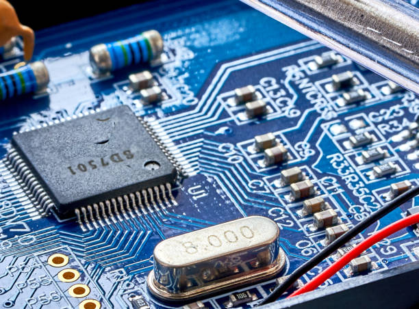
After fabrication, components must be accurately assembled onto the PCB.
A charging power module may combine power semiconductors, controllers, sensors, capacitors, resistors, connectors, and other components. Depending on the design, SMT, through-hole, or mixed-technology assembly may be required.
Reliable PCB assembly should include appropriate process control and inspection to identify issues such as:
- Component placement errors
- Soldering defects
- Insufficient solder joints
- Polarity errors
- Component damage
- Assembly contamination
Depending on product requirements, inspection and testing may include AOI, X-ray inspection, electrical testing, and functional testing.
GOPCBA offers PCB Assembly solutions for different product stages and PCB technologies, helping connect bare-board manufacturing with finished electronic assembly.
8. Prototype Validation Before Production
For new EV charging equipment, prototype development can reveal problems that may not be apparent during schematic or PCB layout review.
A prototype power module can be used to evaluate:
- Current-carrying performance
- Thermal behavior
- Component placement
- Mechanical fit
- Electrical isolation
- Protection circuits
- Communication performance
- Assembly feasibility
Prototype testing is particularly valuable when the design involves high-current paths, new power-conversion architectures, or complex mechanical constraints.
Using Prototype PCB Assembly allows engineers to validate the physical implementation before moving to larger production volumes.
For projects transitioning from engineering samples to pilot manufacturing, Low Volume PCB Assembly can also provide an intermediate production stage for additional validation.
9. Future Trends in EV Charging Power Module PCBs
The continued development of EV charging technology is creating new requirements for PCB design.
Higher charging power, faster charging speeds, intelligent energy management, and increasingly compact equipment can all increase the technical demands placed on power module PCBs.
Future development is likely to focus on:
- Higher current-handling capability
- Improved thermal management
- More compact power architectures
- Better power-conversion efficiency
- Advanced sensing and monitoring
- Improved electromagnetic compatibility
- Greater integration of control and communication functions
- More reliable operation under outdoor conditions
As charging power increases, PCB engineers will need to balance electrical performance, thermal management, manufacturability, reliability, and cost rather than optimizing only one parameter.
Conclusion
The EV charging station PCB is an essential part of the power-conversion and control architecture inside modern charging equipment. Its performance can affect current transmission, thermal behavior, signal communication, and long-term reliability.
A reliable power module PCB should be developed with the complete system in mind—from circuit architecture and PCB power management to material selection, fabrication, assembly, and testing.
By combining appropriate design practices with controlled PCB manufacturing and dependable PCB assembly, EV charging equipment manufacturers can build power modules that are better prepared for high-current operation, demanding outdoor environments, and the continued evolution of fast-charging technology.
:::