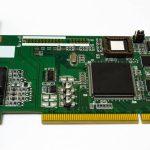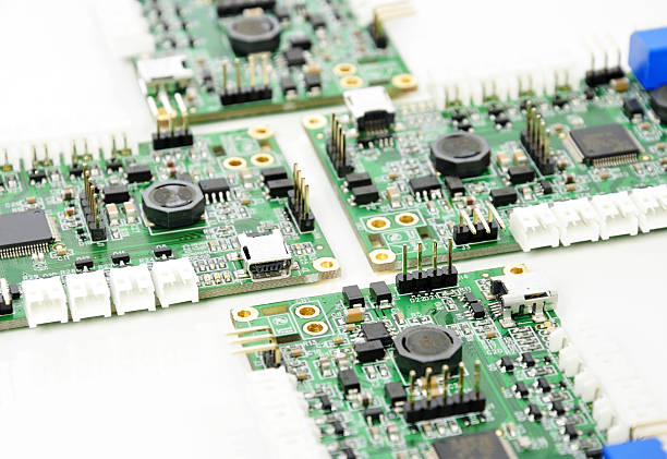
Miniaturized PCB Manufacturing: Precision Processes, Quality Control, and Future Trends
What Is a Miniaturized PCB?
As electronic products continue to become smaller, lighter, and more highly integrated, the demand for miniaturized PCB technology is growing rapidly. Wearable devices, medical electronics, IoT sensors, compact communication equipment, and other space-constrained products require circuit boards that deliver high electrical performance within increasingly limited physical dimensions.
Miniaturization is not simply a matter of reducing board size. It requires tighter control over materials, trace geometry, drilling, layer alignment, solder mask registration, assembly, and inspection.
For manufacturers, miniature PCB manufacturing is therefore a precision-oriented process in which every production stage must be carefully coordinated to achieve the required electrical, mechanical, and reliability performance.
1. Material and Production Preparation
The manufacturing process begins with selecting materials that are compatible with the electrical and mechanical requirements of the application.
For compact and high-density designs, substrate materials need suitable thermal performance, dimensional stability, mechanical strength, and processing characteristics. High-Tg laminate may be considered when the PCB will experience elevated temperatures or demanding assembly conditions.
Copper foil thickness and uniformity are also important. Thinner copper can support finer circuit formation, but the final copper structure must still meet the required current-carrying and reliability requirements.
Before production, manufacturing equipment should be calibrated for the specific board design. High-precision exposure systems, laser drilling equipment, automated optical inspection systems, and other specialized equipment may be required when the design includes fine traces, small vias, or high-density interconnect structures.
Environmental control is equally important. Temperature, humidity, dust, and contamination can affect dimensional stability, surface quality, imaging, and material processing. A controlled production environment helps maintain consistent manufacturing conditions.
For projects requiring engineering review before fabrication, PCB Design & Layout can help establish a manufacturable design foundation.
2. PCB Surface Preparation
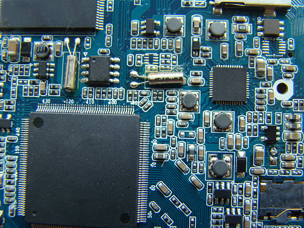
Surface preparation is an essential step before circuit imaging.
The copper surface must be free from oxidation, oil, dust, and other contaminants. Cleaning processes remove surface contamination, while controlled micro-etching can create an appropriate copper surface condition for subsequent dry-film or solder-mask adhesion.
For a fine-line PCB, surface uniformity becomes particularly important because small surface defects can affect the quality of circuit imaging and etching.
After pretreatment, the board should be inspected for scratches, oxidation, contamination, and other defects before entering the circuit-forming process.
3. Fine-Line Circuit Formation
Circuit formation is one of the most critical stages in miniature PCB manufacturing.
A typical process includes:
- Dry-film lamination
- Circuit imaging
- Development
- Copper etching
- Inspection
During dry-film lamination, the film must make uniform contact with the copper surface. Air bubbles, wrinkles, or contamination can cause defects during imaging.
High-precision imaging equipment then transfers the circuit pattern onto the dry film. Accurate registration and controlled exposure energy are essential for maintaining the intended trace geometry.
After development, the exposed copper is etched to form the required circuit pattern. Etching must be carefully controlled because excessive etching can reduce trace width, while insufficient etching can leave unwanted copper between adjacent features.
For fine-line designs, key process parameters may include:
- Etchant concentration
- Etchant temperature
- Spray pressure
- Etching time
- Copper thickness
- Imaging alignment
- Trace width and spacing
Consistent control of these parameters helps reduce variations in line width and improves manufacturing repeatability.
4. Microvia and Small-Hole Processing
As PCB designs become more compact, conventional mechanical drilling may not always be sufficient for every interconnection requirement.
Laser drilling is commonly used for microvias and other small features in high-density PCB structures. The process uses a focused laser beam to remove material and create precisely positioned openings.
After drilling, the hole wall may undergo desmear and metallization processes. Electroless copper deposition followed by electroplating creates a conductive copper layer inside the hole, allowing electrical connections between PCB layers.
Hole quality should be closely monitored. Problems such as insufficient copper coverage, voids, poor alignment, or excessive dimensional variation can negatively affect electrical and long-term reliability.
For high-density applications, manufacturers may also combine microvias with multilayer or HDI structures. GOPCBA’s PCB Manufacturing service supports PCB production for designs ranging from prototypes to more complex production requirements.
5. Miniaturized Solder Mask and Silkscreen Processing
Solder mask protects copper circuits from environmental exposure and helps prevent unintended solder bridging during PCB assembly.
On a compact PCB, solder mask registration must be carefully controlled so that openings align correctly with pads and other solderable areas. The solder mask material should also provide suitable insulation, thermal resistance, and adhesion for the intended application.
Silkscreen printing presents another challenge on small boards. Component references, polarity marks, part numbers, and other identifiers must remain readable without interfering with pads or other critical features.
When space is limited, manufacturers may need to optimize:
- Character size
- Font design
- Ink thickness
- Registration accuracy
- Pad-to-silkscreen clearance
This helps maintain both assembly usability and visual identification.
6. Comprehensive PCB Quality Control
Quality control should extend throughout the entire manufacturing process rather than being limited to final inspection.
Automated optical inspection (AOI) can be used to inspect circuit patterns, solder mask openings, and other visible features. High-resolution imaging helps identify defects such as opens, shorts, line-width deviations, missing features, and registration problems.
For internal structures and vias, X-ray inspection can provide additional information that is not available through conventional visual inspection.
Electrical testing is also important. Depending on the product requirements, testing may include:
- Continuity testing
- Insulation resistance testing
- Dielectric withstand testing
- Electrical resistance testing
- Dimensional inspection
- Visual inspection
For demanding applications, environmental reliability testing can be added to evaluate performance under conditions such as temperature cycling, high temperature and humidity, or other application-specific stresses.
Effective PCB quality control combines process monitoring, automated inspection, electrical testing, and engineering analysis to improve manufacturing consistency.
7. Applications of Miniaturized PCBs
Miniaturized PCBs are increasingly used in products where PCB space is limited but functionality continues to increase.
Wearable Electronics
Smartwatches, fitness trackers, wireless accessories, and other wearable products require compact electronics with efficient use of internal space.
Miniaturized PCB structures can help designers integrate more functions without significantly increasing the overall product size.
Medical Electronics
Medical electronic products often require compact form factors together with high reliability and controlled manufacturing processes.
Depending on the application, manufacturers may need to consider material compatibility, cleanliness, corrosion resistance, electrical reliability, and regulatory requirements.
IoT Devices
IoT sensors and connected devices are often designed around small enclosures and limited power budgets. A compact PCB can integrate sensing, processing, wireless communication, and power-management functions within a restricted area.
For early-stage IoT hardware, Prototype PCB Assembly can be useful for validating PCB design and assembly before larger-scale production.
8. The Role of PCB Assembly in Miniaturized Electronics
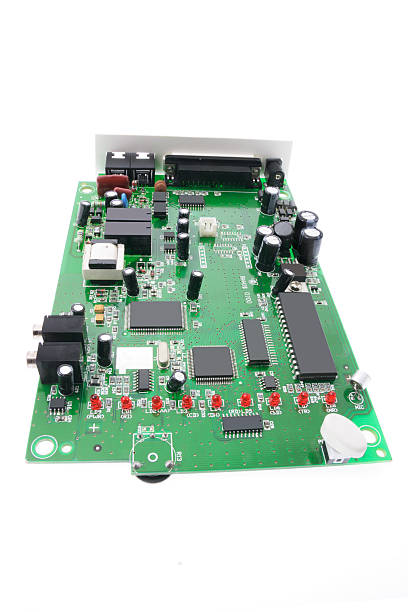
PCB miniaturization does not end with fabrication. Component placement and soldering must also accommodate the smaller board dimensions.
Fine-pitch components, BGA packages, small passive components, and dense component placement can increase assembly complexity. Accurate stencil design, solder paste control, component placement, reflow profiling, and inspection are therefore important.
When the board contains both surface-mount and through-hole components, mixed-technology assembly may require additional process coordination.
GOPCBA’s PCB Assembly service covers PCB assembly requirements across prototype, low-volume, and production applications.
9. Future Trends in PCB Miniaturization
PCB miniaturization is expected to continue as electronic products demand greater functionality in smaller packages.
Several technology trends are particularly important:
Higher-Density Interconnects
HDI structures, microvias, finer traces, and advanced multilayer designs can increase routing density while reducing the space required for electrical interconnections.
Advanced Materials
As operating frequencies, thermal loads, and reliability requirements increase, material selection will become increasingly application-specific. Designers may need to balance dielectric properties, thermal performance, mechanical stability, manufacturability, and cost.
More Precise Manufacturing
Advanced imaging, laser drilling, automated inspection, and process-control technologies will continue to improve manufacturing capability for smaller PCB features.
Intelligent Manufacturing
Automation and digital production management can help monitor process parameters, identify deviations, and improve manufacturing consistency. Data-driven process optimization can also support better traceability and quality analysis.
10. How to Choose a Miniaturized PCB Manufacturer
When selecting a supplier for a miniaturized PCB project, buyers should evaluate more than the quoted unit price.
Important considerations include:
- Fine-line and small-feature manufacturing capability
- Material selection and sourcing
- Layer alignment capability
- Microvia and HDI processing
- Surface-finish options
- Electrical and visual inspection
- PCB assembly capability
- Prototype and low-volume production support
- Engineering and DFM assistance
- Production traceability
- Quality-management systems
A supplier capable of supporting both PCB fabrication and assembly can simplify project coordination and reduce the risks associated with transferring production between multiple vendors.
For projects requiring smaller production quantities, Low Volume PCB Assembly provides an option for validating products before moving toward larger production volumes.
Miniaturized PCB Manufacturing: Key Takeaways
The manufacturing of a miniaturized PCB requires precise coordination across material selection, surface preparation, circuit imaging, fine-line etching, microvia processing, solder mask application, inspection, and electrical testing.
As electronic products become smaller while offering more functions, PCB manufacturers must achieve higher routing density without compromising electrical performance or reliability.
For product developers and procurement teams, the most effective approach is to evaluate PCB manufacturability at the design stage, select materials and processes according to the actual application, and work with a manufacturing partner capable of supporting both PCB fabrication and assembly.
By combining precision PCB manufacturing, robust PCB quality control, and appropriate assembly processes, compact electronic products can achieve the balance between size, functionality, manufacturability, and long-term reliability.