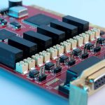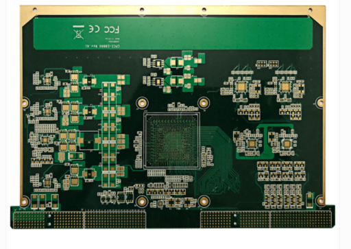
A Multilayer PCB is one of the most important components in modern electronic products. As electronic devices continue to become smaller, faster, and more integrated, multilayer circuit boards are increasingly used to achieve higher routing density, better electrical performance, and more compact product designs.
Unlike single-sided or double-sided circuit boards, a Multilayer PCB integrates multiple conductive layers separated by dielectric materials. These layers may include signal, power, and ground planes, which are interconnected through plated through holes, blind vias, buried vias, and microvias.
Multilayer PCBs are widely used in computers, telecommunications equipment, industrial control systems, automotive electronics, medical devices, aerospace systems, consumer electronics, and high-speed electronic equipment.
The complexity of multilayer board production means that manufacturers must consider much more than simply increasing the number of copper layers. Material selection, circuit design, lamination, drilling, plating, environmental control, and dimensional accuracy all directly influence the quality and reliability of the finished PCB.
For this reason, there are several critical factors that manufacturers should evaluate throughout the PCB Manufacturing Process.
1. Selecting the Appropriate Manufacturing Process
The manufacturing process is one of the most important factors affecting the quality of a Multilayer PCB.
Different circuit boards have different requirements based on their layer count, board thickness, line width and spacing, via structure, material system, copper thickness, and final application.
A conventional multilayer FR-4 board may use a relatively standard manufacturing process, while high-density or high-frequency products may require more advanced technologies.
Important manufacturing processes may include:
- Inner-layer circuit fabrication
- Laser direct imaging
- Mechanical drilling
- Laser drilling
- Desmear
- Electroless copper deposition
- Pattern plating
- Circuit etching
- Sequential lamination
- Via filling
- Solder mask application
- Surface finishing
- Electrical testing
Therefore, manufacturers should select the appropriate PCB Manufacturing Process according to the actual requirements of the board rather than applying the same process to every product.
1.1 Layer Count and Board Structure
Increasing the number of layers can provide additional routing space, but it also increases manufacturing complexity.
As layer count increases, manufacturers need to pay greater attention to:
- Layer-to-layer registration
- Dielectric thickness
- Copper distribution
- Lamination pressure
- Resin flow
- Thermal expansion
- Drilling accuracy
- Via reliability
A well-designed stack-up should balance electrical performance, mechanical stability, manufacturability, and cost.
For high-speed applications, signal layers should be properly referenced to adjacent power or ground planes to provide controlled return-current paths and stable impedance.
1.2 High-Density and Advanced PCB Processes
High-density electronic products may require advanced technologies such as HDI PCB manufacturing, microvias, sequential lamination, and fine-line circuit fabrication.
Compared with conventional multilayer boards, HDI structures can provide higher interconnection density and support smaller component packages.
Laser drilling is commonly used to create microvias, while sequential lamination is used to build additional interconnection layers.
For advanced designs, manufacturers must carefully control:
- Microvia diameter
- Via depth
- Aspect ratio
- Via-to-copper spacing
- Registration accuracy
- Copper plating thickness
- Via filling quality
The selected manufacturing process must therefore be compatible with both the PCB design and the manufacturer’s actual production capabilities.
2. Selecting the Right PCB Materials
Material selection is another fundamental consideration in PCB Fabrication.
PCB substrates can generally be classified into organic and inorganic material systems, with different materials providing different electrical, thermal, mechanical, and processing characteristics.
Common PCB materials include:
- FR-4
- High-Tg FR-4
- High-frequency laminates
- Low-loss materials
- Polyimide
- PTFE-based materials
- BT resin materials
- High-performance composite materials
The appropriate material depends on the intended application.
2.1 Electrical Properties
For high-speed and high-frequency applications, electrical characteristics are particularly important.
Key parameters include:
- Dielectric constant (Dk)
- Dissipation factor (Df)
- Dielectric thickness
- Impedance stability
- Copper surface roughness
Changes in dielectric thickness or dielectric properties can affect controlled impedance and signal transmission.
For High-Frequency PCB applications, low-loss materials may be required to reduce signal attenuation and maintain signal integrity.
2.2 Thermal Properties
Multilayer PCBs used in high-temperature or lead-free assembly environments must withstand repeated thermal stress.
Important thermal parameters include:
- Glass transition temperature (Tg)
- Decomposition temperature (Td)
- Coefficient of thermal expansion (CTE)
- Thermal conductivity
- Z-axis expansion
A material with suitable thermal characteristics can help reduce the risk of delamination, via cracking, and dimensional instability during PCB assembly and operation.
2.3 Copper Foil Thickness
The thickness of the copper foil is another important factor.
Thinner copper foil can make fine-line circuit fabrication easier and may provide better control of narrow trace geometries.
Thicker copper, on the other hand, provides greater current-carrying capability and is often required for power electronics and heavy-copper applications.
However, increasing copper thickness also makes etching and fine-line fabrication more difficult.
Therefore, copper thickness should be selected according to:
- Current requirements
- Trace width and spacing
- Thermal requirements
- Impedance requirements
- Manufacturing capability
3. PCB Lamination Control
PCB Lamination is one of the most critical stages in multilayer board manufacturing.
During lamination, inner-layer circuits, prepreg, and copper foil are stacked according to the specified stack-up and bonded together under controlled temperature and pressure.
The quality of lamination directly affects:
- Interlayer adhesion
- Dielectric thickness
- Layer registration
- Resin distribution
- Void formation
- Dimensional stability
- Thermal reliability
3.1 Resin Flow
Prepreg resin must flow sufficiently during lamination to fill the spaces between copper features and provide reliable bonding.
Insufficient resin flow can lead to voids or poor bonding, while excessive resin flow can cause unwanted dimensional changes and affect dielectric thickness.
The correct lamination parameters depend on the material system, copper pattern, board thickness, and stack-up.
3.2 Layer Registration
As the number of PCB layers increases, layer-to-layer registration becomes increasingly difficult.
Thermal expansion and contraction during lamination can shift internal circuit patterns.
Therefore, manufacturers must use accurate registration systems and appropriate compensation methods to maintain alignment between internal and external layers.
This becomes particularly important for fine-pitch BGA designs, small vias, HDI structures, and high-density multilayer boards.
4. Controlling the PCB Manufacturing Environment
The production environment also has a significant influence on PCB quality.
Temperature and humidity should be appropriately controlled throughout critical manufacturing stages.
Excessive environmental changes may contribute to:
- Material dimensional changes
- Moisture absorption
- Registration variation
- Delamination risks
- Warpage
- Reduced electrical reliability
Moisture is particularly important because many PCB substrate materials are hygroscopic to some degree.
If moisture is absorbed into the laminate, it can expand during high-temperature processes such as lamination or reflow soldering.
This may increase the risk of delamination, blistering, or other thermal reliability problems.
Therefore, manufacturers should establish controlled storage and handling procedures for PCB materials.
5. Drilling and Hole-Wall Quality
Drilling is a critical process in PCB Manufacturing because vias provide electrical connections between different conductive layers.
For multilayer boards, drilling accuracy directly affects interlayer registration and electrical connectivity.
Important drilling factors include:
- Drill diameter
- Spindle speed
- Feed rate
- Drill wear
- Board thickness
- Material construction
- Hole aspect ratio
- Hole position accuracy
Poor drilling conditions may cause:
- Rough hole walls
- Resin smear
- Glass-fiber breakout
- Hole-wall damage
- Excessive burrs
- Dimensional deviations
After drilling, appropriate desmear and hole-wall preparation processes are required before copper deposition.
For HDI boards, laser drilling adds another layer of process complexity because microvia diameter, depth, laser energy, and dielectric characteristics must be carefully controlled.
6. Copper Plating and Interlayer Interconnection
Reliable copper plating is essential for establishing electrical connections between PCB layers.
After drilling, the hole walls are prepared and coated with a conductive copper layer through electroless copper deposition. Subsequent electroplating increases the copper thickness to the required specification.
The quality of plating depends on:
- Hole-wall cleanliness
- Chemical process control
- Current density
- Plating time
- Bath condition
- Copper thickness
- Panel geometry
- Aspect ratio
Uneven copper plating can increase electrical resistance and create potential reliability problems.
For high-reliability multilayer boards, manufacturers should verify copper thickness and plating uniformity through appropriate inspection and cross-sectional analysis.
7. Circuit Fabrication and Etching Accuracy
The circuit pattern must accurately reproduce the PCB design data.
During imaging and etching, trace width and spacing can be affected by exposure conditions, copper thickness, etching rate, compensation, and equipment accuracy.
This is particularly important for fine-line circuits.
Manufacturers should control:
- Trace width
- Trace spacing
- Copper thickness
- Etch compensation
- Line edge quality
- Registration accuracy
For advanced multilayer and HDI applications, technologies such as laser direct imaging and semi-additive processes can provide improved circuit-definition capability.
8. Surface Finishing and Solderability
After circuit fabrication, exposed copper pads require an appropriate surface finish.
Common options include:
- HASL
- Lead-free HASL
- ENIG
- ENEPIG
- OSP
- Immersion silver
- Immersion tin
The appropriate surface finish depends on the PCB design, component pitch, assembly process, storage requirements, and reliability requirements.
For fine-pitch components, a flat surface finish such as ENIG or OSP may be preferred because it provides better control of pad geometry.
Surface finish selection should therefore be considered together with PCB assembly requirements.
9. Manufacturing Equipment and Process Capability
A manufacturer’s equipment capability directly influences the achievable PCB quality.
Modern multilayer PCB production may require:
- High-precision imaging equipment
- CNC drilling machines
- Laser drilling systems
- Automated plating lines
- Lamination presses
- AOI systems
- X-ray inspection equipment
- Electrical testing systems
- Dimensional measurement equipment
However, advanced equipment alone does not guarantee high-quality PCB production.
The manufacturer must also establish suitable process windows, preventive maintenance programs, calibration procedures, statistical process control, and inspection standards.
The actual manufacturing capability should therefore be evaluated based on both equipment and process management.
10. Design for Manufacturability
Good PCB manufacturing begins with a manufacturable design.
During the design stage, engineers should consider the capabilities of the selected PCB manufacturer.
Important DFM considerations include:
- Minimum trace width and spacing
- Minimum via diameter
- Pad dimensions
- Hole aspect ratio
- Copper-to-edge clearance
- Layer registration
- Copper distribution
- Stack-up design
- Impedance requirements
- Surface finish requirements
A design that exceeds manufacturing capability may result in lower yield, higher cost, longer production time, or increased reliability risks.
Therefore, communication between PCB designers and manufacturers should take place before production begins.
11. Quality Inspection and Reliability Verification
Comprehensive inspection is essential for maintaining PCB Quality throughout production.
Depending on the product requirements, manufacturers may use:
- Automated Optical Inspection (AOI)
- Electrical testing
- Flying probe testing
- X-ray inspection
- Microsection analysis
- Solderability testing
- Thermal stress testing
- Dimensional inspection
For high-reliability products, additional reliability tests may be required to evaluate resistance to thermal cycling, moisture, mechanical stress, and long-term electrical operation.
Inspection data can also be used to identify process trends and improve manufacturing consistency.
12. Key Factors at a Glance
The major factors that should be considered when manufacturing a Multilayer PCB can be summarized as follows:
| Factor | Key Considerations |
|---|---|
| Manufacturing Process | Layer count, circuit density, via structure, production capability |
| PCB Materials | Tg, Td, CTE, Dk, Df, moisture absorption |
| Copper Foil | Thickness, current capacity, etching capability |
| PCB Lamination | Resin flow, pressure, temperature, registration |
| Drilling | Hole diameter, position accuracy, hole-wall quality |
| Copper Plating | Thickness, uniformity, adhesion, reliability |
| Circuit Fabrication | Trace width, spacing, etching accuracy |
| Environment | Temperature, humidity, material storage |
| Surface Finish | Solderability, flatness, oxidation resistance |
| Inspection | AOI, electrical testing, X-ray, microsection |
| DFM | Manufacturability, yield, cost, process capability |
13. Kingda’s Approach to Multilayer PCB Manufacturing
Kingda understands that manufacturing a high-quality Multilayer PCB requires coordinated control across materials, equipment, processes, inspection, and engineering.
The manufacturing strategy should begin with a detailed review of PCB design data and material requirements. Manufacturing parameters can then be established according to layer count, board thickness, circuit density, via structure, copper thickness, and electrical requirements.
Kingda focuses on key production controls such as:
- Material selection
- Inner-layer circuit accuracy
- Lamination control
- Drilling precision
- Copper plating uniformity
- Layer registration
- Solder mask accuracy
- Surface finishing
- Electrical testing
- Final inspection
For high-density and high-performance applications, manufacturing processes can be selected according to the actual requirements of the PCB, including HDI structures, fine-line circuits, high-frequency materials, and complex multilayer stack-ups.
This process-oriented approach helps improve manufacturing consistency, production yield, and long-term PCB reliability.
Conclusion
Manufacturing a Multilayer PCB involves considerably more than simply stacking multiple copper layers together.
The final quality of a multilayer circuit board depends on the interaction of PCB Materials, manufacturing processes, lamination, drilling, plating, circuit formation, environmental control, surface finishing, inspection, and design for manufacturability.
Among these factors, material selection and PCB Lamination are particularly important for controlling thermal and mechanical reliability, while drilling, plating, and layer registration directly affect interlayer electrical connections.
For high-density and high-speed applications, manufacturers must also consider advanced requirements such as fine-line fabrication, microvias, controlled impedance, low-loss materials, and HDI PCB manufacturing technologies.
As electronic products continue to move toward higher integration, smaller form factors, faster signal transmission, and greater functional density, multilayer PCB manufacturing will require increasingly precise processes and stricter quality control.
Choosing an experienced PCB manufacturer with appropriate equipment, engineering expertise, and process capability is therefore essential for achieving stable, high-quality, and reliable multilayer circuit boards.