Copper Etching Technology PCB: Process, Principles, and Advantages
Printed circuit boards (PCBs) are essential components in modern electronic products, and their manufacturing technologies continue to evolve to meet increasing performance requirements. Among these technologies, copper etching is one of the most critical processes that directly determines PCB precision, circuit complexity, and overall reliability.
As electronic devices become smaller, faster, and more integrated, advanced Copper Etching Technology PCB solutions have become increasingly important for achieving high-density circuit layouts and stable electrical performance.
Principle of Copper Etching Technology
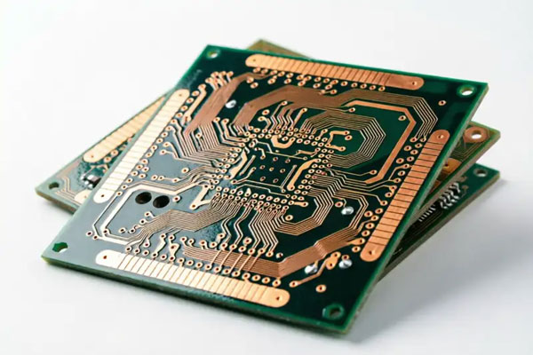
Copper etching is a manufacturing process that selectively removes unwanted copper layers from copper-clad laminates through chemical or physical methods, leaving behind the designed circuit patterns.
The basic principle relies on the chemical reaction between copper and etching solutions. During the process, the exposed copper areas are dissolved, while the protected copper areas remain intact to form the final circuit structure.
In modern PCB Manufacturing Process, etching solutions are mainly divided into two categories: acidic etching solutions and alkaline etching solutions.
Acidic Etching Solution
Copper chloride-hydrochloric acid systems are commonly used acidic etching solutions. Under acidic conditions, copper atoms lose electrons and are oxidized into copper ions. These copper ions dissolve into the solution, gradually removing the unwanted copper layer from the surface.
To maintain stable etching performance, hydrochloric acid concentration must be carefully controlled. Proper chemical balance ensures continuous copper dissolution and improves the accuracy of the Copper Etching Process.
Acidic etching is widely used in traditional PCB manufacturing due to its stable performance, good control capability, and compatibility with various copper-clad materials.
Alkaline Etching Solution
Ammonia-ammonium chloride systems are typical alkaline etching solutions. Under alkaline conditions, copper reacts with ammonia to form stable copper-ammonia complexes, allowing copper to dissolve into the solution.
During production, parameters such as solution concentration, temperature, and pH value must be precisely controlled. Incorrect settings may cause problems such as excessive etching, incomplete copper removal, or reduced circuit accuracy.
For advanced circuit boards, manufacturers must optimize alkaline etching conditions to achieve excellent line definition and maintain the reliability of High Precision PCB manufacturing.
Copper Etching Process in PCB Manufacturing
The complete Copper Etching Process involves several important stages. Each step directly affects the quality, accuracy, and reliability of the final PCB.
Resist Layer Formation
Before copper etching begins, a protective resist layer must be created on the surface of the copper-clad laminate.
Common resist materials include photoresist and dry film. Photoresist uses photolithography technology to transfer the designed circuit pattern onto the copper surface through ultraviolet exposure and development.
Dry film is another widely used method. It is laminated onto the copper surface through heat pressing and then exposed and developed to create a precise protective pattern.
The accuracy and integrity of the resist layer determine the final circuit pattern quality. A high-quality resist process is essential for producing advanced Multilayer PCB products with fine lines and complex structures.
Copper Etching Process
After the resist layer is completed, the PCB panel enters the etching equipment where it contacts the etching solution.
During this stage, the exposed copper areas react with the chemical solution and gradually dissolve. The etching equipment must precisely control several parameters, including:
- Etching solution temperature
- Chemical concentration
- Solution flow rate
- Etching duration
The temperature directly affects reaction speed. Excessive temperature may cause uneven etching, while insufficient temperature reduces production efficiency.
A stable solution flow ensures fresh etching chemicals continuously reach the copper surface, improving consistency.
Accurate etching time control is also essential. Over-etching may damage circuit traces, while under-etching can leave unwanted copper residues and create short circuit risks.
Resist Removal
After etching is completed, the protective resist layer must be removed to expose the finished copper circuit pattern.
Photoresist is generally removed using specialized stripping chemicals, while dry film can be removed through chemical or mechanical stripping methods.
After resist removal, the PCB surface undergoes cleaning and drying processes to eliminate residues and prepare the board for subsequent manufacturing stages.
For advanced PCB Manufacturing Process requirements, proper cleaning after etching is critical to ensuring long-term electrical reliability.
Advantages of Copper Etching Technology in PCB Manufacturing
High Precision Circuit Formation
With the rapid development of compact and high-performance electronic products, PCB manufacturers require increasingly precise circuit patterns.
Advanced copper etching technology enables the production of extremely fine circuit structures, supporting high-density designs used in smartphones, computers, communication devices, and industrial electronics.
Through optimized etching control, manufacturers can achieve narrow line widths and spacing at the micron level, improving circuit integration and signal transmission performance.
This capability makes copper etching a fundamental technology for High Precision PCB manufacturing.
Ability to Create Complex Circuit Patterns
Modern electronic products require increasingly complex circuit designs, including multilayer structures, high-density interconnections, and specialized layouts.
Copper etching technology can accurately transfer complex circuit designs from engineering data into physical PCB patterns.
Whether manufacturing advanced Multilayer PCB structures or supporting compact electronic systems, precise etching technology enables designers to achieve greater functional integration.
Excellent Consistency and Reliability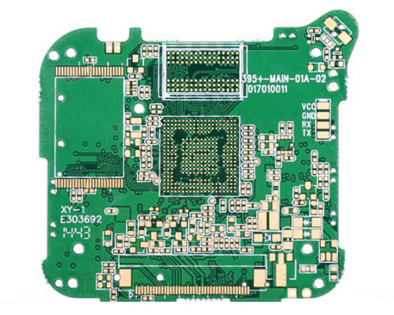
In large-scale PCB production, process consistency is one of the most important quality requirements.
By accurately controlling etching parameters such as chemical composition, temperature, flow rate, and processing time, manufacturers can maintain stable results across different production batches.
Consistent copper etching reduces manufacturing defects, improves production efficiency, and enhances product reliability.
For applications requiring strict quality standards, selecting a professional PCB Manufacturing Service provider helps ensure stable process control and reliable circuit performance.
Applications of Copper Etching Technology
Copper etching technology is widely used across multiple industries, including:
Consumer Electronics
Smartphones, tablets, laptops, and wearable devices require compact and highly integrated PCBs.
Copper etching enables manufacturers to create fine circuit patterns within limited spaces, supporting lightweight designs and advanced electronic functions.
Communication Equipment
High-speed communication systems require PCBs with excellent signal integrity and precise circuit structures.
Copper etching technology supports the production of high-frequency and high-density circuit boards used in communication infrastructure, networking equipment, and wireless devices.
Automotive Electronics
Modern vehicles rely on complex electronic systems, including battery management systems, autonomous driving modules, and vehicle control units.
Reliable copper etching technology ensures stable circuit performance under demanding automotive environments involving temperature changes, vibration, and long operating cycles.
Medical Equipment
Medical devices require extremely reliable PCB solutions because signal accuracy and operational stability directly affect equipment performance.
High-precision copper etching supports medical imaging systems, monitoring devices, and diagnostic equipment by providing accurate circuit structures and dependable electrical connections.
Future Development of Copper Etching Technology
As electronic products continue moving toward higher integration, faster transmission speeds, and smaller dimensions, copper etching technology will continue evolving.
Future development trends include:
- More advanced fine-line etching technology
- Improved control of micro-scale circuit patterns
- Environmentally friendly etching chemicals
- Higher automation and intelligent manufacturing processes
Manufacturers will continue optimizing etching accuracy and process stability to meet the growing demand for advanced PCB solutions.
Copper etching technology remains one of the core technologies driving PCB innovation. Through continuous improvements in materials, equipment, and process control, it will continue supporting the development of next-generation electronic products with higher performance, smaller size, and greater reliability.