ENIG PCB vs HASL PCB to Complete Comparison Guide
In modern PCB surface finish technology, the treatment applied to exposed copper pads plays an important role in solderability, corrosion resistance, assembly performance, and product reliability. Among the commonly used surface finishing options, ENIG PCB and HASL PCB are two widely adopted technologies.
Although both processes are designed to protect exposed copper and provide a suitable surface for component soldering, their manufacturing principles, surface characteristics, cost structures, and application areas are significantly different.
Understanding the differences between ENIG vs HASL can help engineers and purchasing teams select the most appropriate finish according to PCB design requirements, component package type, assembly process, operating environment, production volume, and budget.
What Is the Difference Between ENIG and HASL?
The fundamental difference between ENIG and HASL lies in how the protective layer is created on the exposed copper surface.
How ENIG PCB Surface Finish Works
ENIG stands for Electroless Nickel Immersion Gold. It uses a chemical deposition process to create a nickel-gold protective structure on exposed copper.
First, an electroless nickel layer is deposited onto the copper pad. A thin layer of immersion gold is then deposited over the nickel layer through a chemical displacement reaction.
The resulting structure can be described as a nickel barrier layer with a gold surface layer. The nickel provides mechanical protection and acts as a barrier between copper and gold, while the gold protects the surface against oxidation and provides a stable soldering surface.
Because the process does not depend on electrical current for nickel deposition, the resulting surface can be relatively uniform and flat across exposed copper areas.
How HASL PCB Surface Finish Works
HASL stands for Hot Air Solder Leveling. Unlike ENIG, HASL is primarily a thermal and physical coating process.
During HASL processing, the PCB surface is cleaned and prepared before the board passes through molten solder. High-pressure hot air knives are then used to remove excess solder and level the coating across the exposed copper pads.
Traditional HASL commonly used lead-containing solder alloys. Today, lead-free HASL is widely used where compliance with environmental requirements is necessary.
The fundamental distinction is therefore straightforward: ENIG creates a controlled nickel-gold chemical coating, while HASL applies a molten solder coating and uses hot air to level the surface.
ENIG vs HASL: Key Performance Differences
The choice between ENIG PCB and HASL PCB should be based on the technical requirements of the finished circuit board rather than simply on price.
Surface Flatness and SMT Compatibility
One of the most significant advantages of ENIG is its excellent surface flatness.
The chemical deposition process produces a relatively smooth and uniform surface, making ENIG particularly suitable for high-density PCB designs and fine-pitch components.
This characteristic is especially valuable for BGA packages and other components with closely spaced solder pads. A consistent pad surface can support more predictable solder paste deposition and component placement during SMT assembly.
For compact electronics, wearable devices, communication equipment, and other products using fine-pitch components, ENIG can provide an important manufacturing advantage.
HASL generally produces a less uniform surface because molten solder solidifies after the leveling process. Small variations in solder thickness or pad topography may occur.
For large pads and conventional components, this typically presents few problems. However, for extremely fine-pitch packages, surface variations can make component placement and solder paste printing more challenging.
For complex PCB production and assembly requirements, surface finish selection should therefore be evaluated together with the overall PCB Manufacturing process.
Corrosion Resistance and Storage Life
Gold has excellent chemical stability, which contributes to the corrosion resistance of ENIG.
The gold surface helps protect the underlying nickel and copper from oxidation and environmental exposure. As a result, ENIG boards can maintain a stable solderable surface during storage when properly manufactured, packaged, and handled.
This characteristic is useful for products with longer manufacturing cycles or applications where PCB storage time may be relatively long.
HASL relies primarily on its solder coating for surface protection. Over time, the exposed solder surface can oxidize, particularly when boards are stored under unfavorable environmental conditions.
Therefore, HASL boards generally require appropriate storage and handling procedures to preserve solderability before assembly.
Solderability and Assembly Compatibility
Both ENIG and HASL can provide good solderability when the PCB surface finish is properly manufactured and controlled.
ENIG offers a smooth and consistent surface that works well with automated SMT assembly and fine-pitch components. The gold layer protects the nickel surface before soldering, while the soldering process allows the joint to form with the underlying metallic structure.
HASL also provides good initial solderability. Because the exposed pads are coated with solder, the surface can readily interact with solder during assembly.
However, lead-free HASL typically requires higher processing temperatures than traditional lead-containing HASL. This can increase thermal stress on thin PCBs and some sensitive structures.
For prototype projects where design changes and repeated assembly cycles are expected, engineers can also consider Prototype PCB Assembly to validate the selected surface finish and assembly process before production.
Cost Considerations
Cost is another major difference between ENIG and HASL.
ENIG generally has a higher manufacturing cost because it requires additional chemical processing and the use of nickel and gold layers. The process also requires tighter control of plating conditions.
HASL is generally more economical and is therefore widely used for applications where extreme surface flatness and long-term surface stability are not primary requirements.
For high-volume products with conventional component packages and cost-sensitive designs, HASL can provide an effective balance between manufacturing cost and soldering performance.
For high-density or higher-reliability electronics, the additional cost of ENIG may be justified by its surface flatness, corrosion resistance, and assembly advantages.
ENIG vs HASL: Application Differences
Neither ENIG nor HASL is universally better. Each surface finish is optimized for different application requirements.
Applications of ENIG PCB
ENIG is commonly considered for applications where surface flatness, fine-pitch assembly, corrosion resistance, and stable solderability are important.
Typical applications include:
- High-density electronic equipment
- Telecommunications equipment
- 5G communication hardware
- BGA-based circuit boards
- High-end consumer electronics
- Wearable electronic devices
- Industrial control electronics
- Medical electronics
- Aerospace and other high-reliability electronics
For advanced products with dense routing and complex component placement, ENIG can be particularly suitable.
When ENIG is combined with high-density PCB structures and controlled manufacturing processes, it can support the assembly requirements of increasingly compact electronic products.
Applications of HASL PCB
HASL is commonly used when cost efficiency and conventional soldering performance are the primary considerations.
Typical applications include:
- Consumer electronics
- Household appliances
- Conventional control boards
- Standard double-sided PCBs
- Industrial control equipment
- Cost-sensitive electronic products
- Applications using relatively large-pitch components
Lead-free HASL can also be used in applications where environmental requirements need to be considered while maintaining a relatively economical PCB manufacturing process.
ENIG vs HASL: Advantages and Disadvantages
Advantages of ENIG PCB
The main advantages of ENIG include:
- Excellent surface flatness
- Good compatibility with fine-pitch components
- Suitable for BGA assembly
- Good corrosion resistance
- Stable surface condition
- Good storage characteristics
- Suitable for high-density PCB designs
- Consistent surface appearance
The primary disadvantage is its higher manufacturing cost compared with HASL.
Advantages of HASL PCB
The main advantages of HASL include:
- Lower manufacturing cost
- Good initial solderability
- Suitable for conventional SMT assembly
- Suitable for through-hole soldering
- Widely available manufacturing process
- Good choice for cost-sensitive applications
Its main limitation is that the surface is generally less flat than ENIG, which can make it less suitable for some fine-pitch and high-density applications.
How to Choose Between ENIG and HASL
Selecting the right PCB surface finishing technology requires consideration of the entire product design and manufacturing process.
Consider Component Package Requirements
If the board contains BGA, fine-pitch ICs, or other components with closely spaced pads, ENIG is often a more suitable option because of its relatively flat and uniform surface.
For conventional components with larger pad spacing, HASL may provide sufficient performance at a lower cost.
Consider the PCB Assembly Process
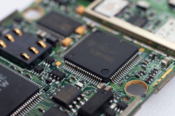
The selected surface finish should be compatible with the intended assembly technology.
SMT assembly, through-hole assembly, mixed-technology assembly, solder paste printing, component placement, and reflow soldering can all influence the optimal finish.
For complex assemblies combining different component technologies, Mixed Technology PCB Assembly can be integrated with the PCB manufacturing process to evaluate the complete assembly requirements.
Consider Storage and Operating Environment
Environmental conditions should also influence the choice.
For products requiring longer storage periods or improved resistance to oxidation and corrosion, ENIG can provide advantages.
For products manufactured and assembled within a relatively short period, HASL may provide a more economical solution when its surface characteristics meet the design requirements.
Consider Production Cost and Volume
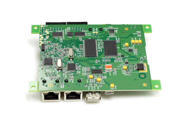
Cost becomes increasingly important as production volume increases.
For cost-sensitive high-volume products using conventional components, HASL can be an attractive option.
For advanced electronic products where assembly reliability and surface flatness are more important than minimum unit cost, ENIG may provide better overall value.
For production programs that move from engineering samples to larger production quantities, High Volume PCB Assembly can be considered as part of the overall manufacturing strategy.
ENIG vs HASL: Which One Should You Choose?
There is no universal answer when comparing ENIG vs HASL. The optimal choice depends on the PCB’s design, component density, assembly technology, environmental conditions, expected storage period, production volume, and target cost.
Choose ENIG when you need:
- A flat and uniform PCB surface
- Fine-pitch component compatibility
- BGA assembly support
- Better corrosion resistance
- Longer surface stability
- High-density PCB assembly
- Higher reliability for demanding applications
Choose HASL when you prioritize:
- Lower PCB manufacturing cost
- Conventional component assembly
- Good basic solderability
- Cost-sensitive production
- Standard PCB applications
- Large or medium pad geometries
In other words, ENIG is generally more appropriate when precision and surface performance are priorities, while HASL remains an economical choice for many conventional electronic products.
The Importance of Professional PCB Surface Finishing
The performance of a surface finish depends not only on the selected technology but also on the quality of the underlying PCB manufacturing process.
Copper preparation, plating control, solder mask quality, pad design, surface cleanliness, process parameters, inspection, and final assembly all influence the reliability of the finished board.
For demanding projects, engineers should evaluate surface finish selection during the PCB design stage rather than treating it as a final manufacturing decision.
A complete manufacturing workflow can connect PCB design, fabrication, component sourcing, assembly, inspection, and testing. This approach helps ensure that the selected surface finish is compatible with the complete production process.
For customers looking for an integrated manufacturing solution, Turnkey PCB Assembly can combine PCB fabrication, component sourcing, assembly, and testing into a coordinated production workflow.
Conclusion
ENIG PCB and HASL PCB are both established PCB surface finish technologies, but they address different manufacturing priorities.
ENIG provides excellent surface flatness, good corrosion resistance, stable solderability, and strong compatibility with fine-pitch and high-density PCB assembly. These characteristics make it a strong choice for advanced electronic products where assembly precision and reliability are important.
HASL offers good solderability at a lower cost and remains a practical solution for conventional electronic products, especially where component spacing is relatively large and extreme surface flatness is not required.
The best approach to ENIG vs HASL selection is to evaluate the complete application rather than focusing on a single parameter. By considering component packages, PCB design, assembly technology, operating environment, storage requirements, production volume, and cost targets together, engineers can select the most appropriate PCB surface finishing technology for the project.