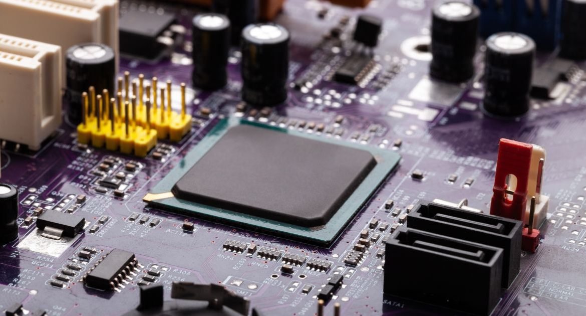
Not every electronics project requires the same manufacturing technology. When selecting a PCB manufacturing method, factors such as development time, production volume, board complexity, design requirements, and overall cost all need to be considered.
For many electronics products, PCB prototyping is an essential step between circuit design and final production. A prototype allows engineers to verify electrical performance, mechanical dimensions, component placement, signal integrity, thermal behavior, and manufacturability before committing to larger production volumes.
During this stage, multiple design iterations may be required. Engineers can fabricate, assemble, test, and modify prototype boards until the design achieves the required performance.
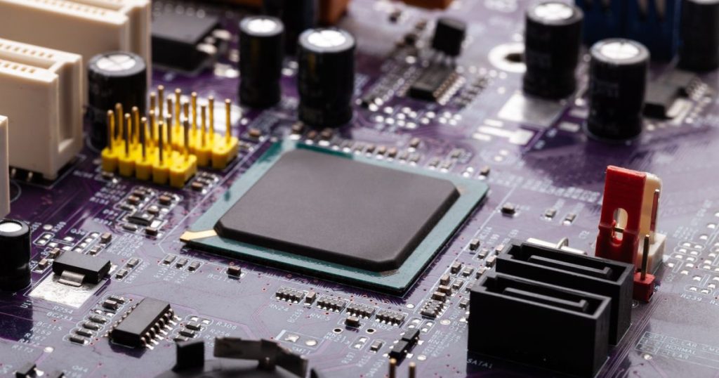
Traditional PCB prototyping remains the preferred solution for most commercial electronics applications. However, additive manufacturing, more commonly known as 3D printing, has introduced another option for certain low-volume and highly customized electronic designs.
The key question is not whether additive manufacturing is better than conventional PCB manufacturing. Instead, the right choice depends on the specific requirements of the project.
Kingda supports customers with PCB manufacturing, rapid PCB prototyping, and PCB assembly, helping engineering teams evaluate manufacturing requirements and move from prototype development to reliable production.
PCB Additive Manufacturing vs. Traditional PCB Manufacturing
Before selecting a manufacturing method, engineers should consider several important questions:
- Is the project low-volume or high-volume?
- How complex is the circuit design?
- Are custom or non-planar geometries required?
- How quickly are prototypes needed?
- Does the design require specialized materials?
- Will the prototype eventually move into mass production?
- Are tooling costs a major concern?
- Does the project require PCB assembly and testing?
- What level of reliability is required?
These questions help determine whether 3D printed PCB technology, conventional PCB fabrication, or a combination of both is the most appropriate approach.
Traditional PCB Manufacturing
Conventional PCB manufacturing generally uses established processes such as imaging, etching, drilling, plating, lamination, solder mask application, and surface finishing.
These processes are highly optimized for commercial production and are particularly suitable for:
- Multilayer PCBs
- HDI circuit boards
- High-volume production
- High-reliability electronics
- Fine-pitch components
- Controlled impedance designs
- Automotive electronics
- Medical electronics
- Industrial equipment
- Telecommunications systems
Traditional PCB fabrication provides predictable electrical and mechanical characteristics and is supported by mature quality-control and inspection technologies.
PCB Additive Manufacturing
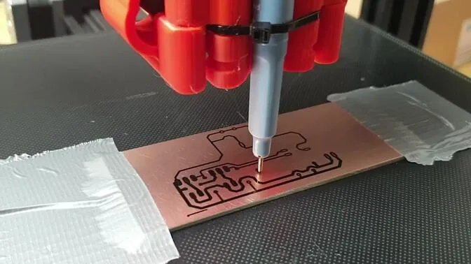
Additive PCB manufacturing builds conductive and dielectric structures by depositing materials layer by layer based on digital design data.
Instead of removing unwanted copper from a larger copper-clad substrate, additive processes selectively deposit conductive or insulating materials to create the required circuit structure.
This approach can be attractive for highly customized designs, low-volume applications, and certain rapid-development scenarios where conventional tooling or fabrication steps would add significant time.
However, additive manufacturing does not replace traditional PCB fabrication for every application. Conventional manufacturing remains more practical for many multilayer, high-volume, and high-reliability PCB applications.
How Does PCB Additive Manufacturing Work?
Additive manufacturing creates a physical structure from digital design information by depositing material progressively, layer by layer.
For electronic applications, the digital circuit design is first converted into manufacturing data that defines conductive paths, dielectric structures, interconnections, and other features.
Depending on the technology, additive PCB manufacturing may use processes such as:
- Inkjet-style material deposition
- Aerosol or direct-write printing
- Conductive ink deposition
- 3D extrusion
- Multi-material additive manufacturing
- Laser-assisted deposition
The specific process depends on the required conductor geometry, substrate material, electrical characteristics, and intended application.
2D Printed Electronics
Some additive electronic manufacturing technologies deposit conductive materials onto a relatively flat substrate.
This approach can be useful for applications requiring:
- Printed conductive traces
- Sensors
- Antennas
- Flexible electronic structures
- Low-volume electronic prototypes
- Customized conductive patterns
Because the conductive material is deposited directly where it is required, material waste can potentially be reduced compared with some conventional subtractive processes.
3D Printed Circuit Structures
More advanced additive technologies can create electronic structures with three-dimensional geometries.
Instead of limiting conductive traces to conventional flat PCB layers, designers may be able to integrate conductive paths into or onto non-planar structures.
Potential applications include:
- Customized sensors
- Embedded electronics
- Wearable devices
- Antenna structures
- Compact electromechanical systems
- Specialized prototypes
This capability provides designers with additional freedom when developing products that cannot easily be implemented using traditional planar PCB structures.
How Additive Manufacturing Can Reduce PCB Prototype Lead Time
One of the major attractions of additive manufacturing is the potential to shorten prototype development time.
Traditional PCB prototyping may involve multiple manufacturing stages, including tooling, imaging, drilling, plating, etching, solder mask application, surface finishing, and inspection.
For certain additive processes, fewer manufacturing steps may be required because the digital design can be translated directly into a physical structure.
Potential advantages include:
Digital Manufacturing Workflow
A digitally controlled process can reduce manual intervention and simplify the transition from design data to prototype production.
This can be particularly useful when engineers need to evaluate several design concepts within a short development cycle.
Low-Volume Flexibility
Additive manufacturing can be attractive when only a small number of experimental boards or conductive structures are required.
Instead of establishing a large production setup for a very small quantity, engineers may be able to produce the required structures directly from digital manufacturing data.
Reduced Tooling Requirements
Some additive processes can reduce or eliminate certain dedicated tooling requirements.
This can make the technology attractive for experimental designs, highly customized components, and early-stage product development.
However, tooling requirements vary significantly between manufacturing technologies. Conventional PCB manufacturing can also provide highly cost-effective prototypes when the board structure and order quantity are suitable.
Traditional PCB Prototyping Still Has Major Advantages
Although additive manufacturing provides exciting possibilities, conventional PCB prototyping remains the standard choice for many electronic products.
This is because traditional PCB fabrication offers a mature combination of electrical performance, material availability, manufacturing consistency, and scalability.
For example, conventional PCB manufacturing can support advanced materials and structures such as:
- FR-4 multilayer PCBs
- High-Tg PCB materials
- High-frequency laminates
- Flexible PCBs
- Rigid-flex PCBs
- HDI PCBs
- Microvias
- Blind and buried vias
- Controlled impedance structures
- Heavy copper PCBs
- High-voltage PCB designs
These technologies are widely used in commercial and industrial electronics where reliability and repeatability are essential.
For products that eventually require hundreds, thousands, or millions of boards, it is generally more practical to develop the prototype using a manufacturing process that can transition efficiently into production.
Greater Design Freedom With Additive PCB Manufacturing
One of the most interesting advantages of additive manufacturing is its potential to expand design freedom beyond conventional planar PCB geometry.
Traditional PCB design is primarily based on flat layers stacked together. Although modern technologies such as HDI and rigid-flex provide considerable flexibility, designers still need to work within established manufacturing constraints.
Additive manufacturing can potentially support more complex geometries, including:
- Curved conductive paths
- Three-dimensional structures
- Variable thicknesses
- Embedded conductive elements
- Customized surface topographies
- Non-planar electronic assemblies
This can be valuable for specialized products where the PCB itself must conform to a particular mechanical shape.
For example, a sensor integrated into a curved housing may benefit from a non-planar electronic structure rather than a conventional rectangular PCB.
However, increased design freedom also introduces new engineering challenges. Electrical performance, thermal behavior, mechanical strength, material compatibility, and long-term reliability must all be evaluated before the technology is used in production.
Why Prototype Testing Remains Essential
Regardless of whether a prototype is produced using additive manufacturing or conventional PCB fabrication, prototype testing remains essential.
A prototype should be evaluated for more than basic electrical functionality.
Depending on the application, testing may include:
- Electrical continuity testing
- Insulation resistance testing
- Functional testing
- Signal integrity testing
- Impedance testing
- Thermal testing
- Mechanical fit testing
- Environmental testing
- Solderability evaluation
- Assembly validation
For assembled prototypes, inspection technologies such as AOI (Automated Optical Inspection), SPI (Solder Paste Inspection), and X-ray inspection can also be used when appropriate.
The purpose of prototyping is not simply to prove that the circuit works. It is also to determine whether the design can be manufactured consistently and economically.
How Kingda Supports Rapid PCB Prototyping
For most commercial electronics projects, the transition from prototype to production is more important than simply producing a prototype as quickly as possible.
Kingda provides rapid PCB prototyping and PCB manufacturing services to help customers validate designs and prepare them for production.
Kingda’s approach can include:
Design Review and DFM
Before manufacturing begins, engineers can review the PCB design for manufacturability issues involving trace width, spacing, drill sizes, copper distribution, layer stack-up, component placement, and other fabrication requirements.
Rapid PCB Prototype Manufacturing
Prototype PCBs allow engineers to evaluate their designs before moving into larger production quantities.
PCB Assembly
Kingda can combine PCB fabrication with PCB assembly, including SMT and through-hole assembly, allowing customers to evaluate the complete electronic assembly rather than only the bare board.
Testing and Inspection
Prototype assemblies can be inspected and tested to identify potential design or manufacturing problems before production scaling.
Production Transition
Once the design has been validated, the manufacturing process can transition toward repeatable production, reducing the need to transfer the project to a completely different supplier.
PCB Prototype and PCB Assembly From One Manufacturing Partner
A PCB prototype is often only one component of a larger product-development process.
After the bare PCB has been fabricated, components must be sourced and assembled before engineers can fully evaluate the electronic product.
This makes an integrated PCB manufacturing and PCB assembly service particularly valuable.
Kingda can support a workflow such as:
PCB Design → DFM Review → PCB Prototype → Component Sourcing → SMT Assembly → Through-Hole Assembly → Inspection → Testing → Production
This integrated model can provide several benefits:
- Simplified supplier management
- Better communication
- Reduced logistics complexity
- Faster engineering feedback
- Improved manufacturing consistency
- Easier prototype-to-production transition
For companies developing new electronic products, working with a partner that understands both bare-board fabrication and assembly requirements can reduce communication gaps between PCB design and final product development.
Where 3D Printing Can Complement Traditional PCB Manufacturing
Additive manufacturing does not have to compete directly with conventional PCB fabrication.
In many cases, 3D printing can complement traditional PCB manufacturing by producing mechanical parts, fixtures, tooling, and prototypes used during PCB development and assembly.
Prototype Enclosures
Engineers can use 3D printing to quickly produce an enclosure and verify the physical relationship between the PCB, components, connectors, and housing.
Assembly Fixtures and Jigs
Customized fixtures can help position components, labels, cables, connectors, or PCBs during assembly.
Protective Components
Small protective caps and covers can be produced for specific manufacturing operations, including processes involving conformal coating.
Alignment Tools
Customized alignment tools can help improve repeatability during assembly and testing.
Manufacturing Aids
3D-printed manufacturing aids can sometimes replace outsourced low-volume tooling, especially when a customized fixture is needed quickly.
These applications demonstrate that additive manufacturing can provide value even when the actual PCB continues to be produced using conventional fabrication technology.
Additive Manufacturing vs. Traditional PCB Manufacturing
The following comparison provides a practical overview:
| Factor | Additive PCB Manufacturing | Traditional PCB Manufacturing |
|---|---|---|
| Prototype Speed | Potentially very fast for suitable designs | Fast with dedicated prototype services |
| Tooling | May require minimal tooling | Tooling may be required depending on process |
| Low Volume | Highly suitable for some applications | Also suitable through prototype processes |
| High Volume | Limited for many current applications | Highly suitable |
| Complex Geometry | Excellent potential | Primarily planar, with advanced rigid-flex options |
| Material Selection | Depends on additive technology | Very broad material ecosystem |
| HDI Technology | Technology-dependent | Mature HDI manufacturing processes |
| Production Scalability | Application-dependent | Excellent |
| Reliability Data | Technology-dependent | Extensive industry experience |
| PCB Assembly | Usually requires additional processes | Widely integrated with PCBA services |
The most appropriate technology depends on the product’s electrical, mechanical, manufacturing, and commercial requirements.
When Should You Choose Additive PCB Manufacturing?
Additive manufacturing may be worth considering when a project has one or more of the following characteristics:
- Extremely low production volume
- Highly customized electronic structures
- Complex three-dimensional geometry
- Rapid experimental development
- Limited tooling budget
- Specialized sensors or antennas
- Non-planar electronic requirements
- Research and development applications
However, additive manufacturing should not be selected solely because it is faster.
Engineers should also consider electrical performance, material properties, thermal management, reliability, assembly compatibility, certification requirements, and the expected production volume.
When Is Traditional PCB Manufacturing the Better Choice?
Traditional PCB manufacturing is generally the more practical option when the project requires:
- High production volumes
- Multilayer PCB structures
- HDI circuit boards
- High-reliability applications
- Established laminate materials
- Fine-pitch SMT assembly
- Controlled impedance
- Consistent electrical performance
- Automotive, medical, industrial, or telecommunications applications
- A clear path from prototype to mass production
For these projects, an experienced PCB manufacturer can provide a more mature and scalable manufacturing solution.
Kingda’s Advantage in PCB Prototyping and Manufacturing
Kingda focuses on helping customers move efficiently from PCB design to functional prototypes and production-ready electronic assemblies.
Key advantages include:
Rapid PCB Prototyping
Kingda supports rapid PCB prototyping to help engineers validate new designs, identify manufacturing issues, and shorten development cycles.
Professional PCB Manufacturing
Kingda provides customized PCB manufacturing solutions for different board structures, materials, layer counts, and technical requirements.
HDI and Advanced PCB Technology
For compact and high-density electronic products, Kingda can support advanced HDI PCB requirements, including sophisticated multilayer structures and microvia technologies where applicable.
PCB Assembly Integration
With PCB assembly capabilities, Kingda can support both bare PCB fabrication and assembled circuit boards, helping customers reduce supplier coordination.
DFM Engineering Support
Design-for-manufacturing review helps identify potential fabrication and assembly issues before production, reducing unnecessary redesigns and manufacturing risks.
Prototype-to-Production Support
Kingda can support customers beyond the prototype stage, helping transition validated designs into repeatable production.
One-Stop Manufacturing Solution
By combining PCB fabrication, PCB prototyping, component sourcing, PCB assembly, inspection, and testing, Kingda provides an integrated manufacturing solution for electronics developers and OEM customers.
Conclusion
PCB additive manufacturing and traditional PCB manufacturing are not competing technologies in every situation. Each has its own strengths, limitations, and ideal applications.
Additive manufacturing can provide significant advantages for highly customized, low-volume, experimental, and three-dimensional electronic structures. It can also complement traditional PCB production by providing rapid mechanical fixtures, enclosures, tooling, and other manufacturing aids.
Traditional PCB fabrication, however, remains the preferred approach for most commercial electronic products that require established materials, multilayer structures, HDI technology, reliable assembly, scalable production, and consistent quality.
For companies developing new electronic products, the most effective strategy is to select the manufacturing technology according to the project’s actual requirements rather than focusing exclusively on prototype speed.
Kingda combines PCB manufacturing, rapid PCB prototyping, HDI PCB technology, and PCB assembly to support customers throughout the product development cycle. From design review and prototype fabrication to assembly, testing, and production, Kingda provides an integrated approach designed to make PCB development more efficient and scalable.