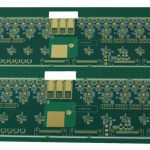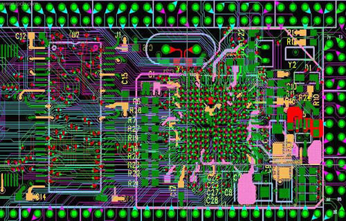
A PCB Via is one of the most important structural elements in a multilayer printed circuit board. Vias provide electrical connections between different copper layers and can also serve mechanical or positioning purposes during PCB manufacturing and assembly.
Drilling is a significant part of the PCB fabrication process, and drilling-related operations can account for a considerable portion of total manufacturing cost, particularly for high-density and multilayer boards.
From a functional perspective, PCB holes can generally be divided into two categories:
- Holes used for electrical interconnection between PCB layers
- Holes used for mechanical mounting, positioning, or assembly
From a manufacturing perspective, interconnection vias are generally classified as Through-Hole, Blind Via, and Buried Via structures.
Understanding these via types and their electrical characteristics is particularly important for High-Speed PCB Design, because vias introduce parasitic capacitance, parasitic inductance, and impedance discontinuities that can affect signal integrity.
1. Basic Types of PCB Vias
1.1 Through-Hole Via
A Through-Hole via passes completely through the PCB from one side to the other.
The plated hole can electrically connect multiple signal, power, or ground layers.
Through-holes can also be used for through-hole component leads, mechanical mounting, and positioning, depending on the PCB design.
Because through-hole vias are relatively simple to manufacture, they are widely used in conventional multilayer PCB fabrication.
Their major advantages include:
- Simple manufacturing process
- Lower fabrication cost
- High manufacturing reliability
- Compatibility with conventional PCB processes
- Ability to connect multiple PCB layers
However, the main disadvantage is that the entire hole barrel occupies routing space on every layer it passes through.
For high-density PCB layouts, this can significantly reduce available routing space.
1.2 Blind Via
A Blind Via connects an outer PCB layer to one or more inner layers but does not pass completely through the board.
Blind vias are commonly used to connect:
- Top layer to inner layer
- Bottom layer to inner layer
Because blind vias do not extend through the entire PCB, they occupy less routing space than conventional through-hole vias.
They are particularly useful for high-density designs and fine-pitch components.
Blind vias are commonly manufactured using controlled-depth drilling or laser drilling, depending on the PCB structure and required feature size.
1.3 Buried Via
A Buried Via is located entirely inside the PCB stack-up and connects internal copper layers without extending to either outer surface.
Buried vias are fabricated within selected multilayer structures before the complete PCB stack-up is laminated.
They provide additional routing flexibility because the via does not occupy space on the outer layers.
However, buried vias require more complex fabrication processes and generally cost more than conventional through-hole vias.
1.4 Microvia
A Microvia is a very small via structure commonly associated with HDI (High-Density Interconnect) PCB technology.
Microvias are typically produced using laser drilling and are generally used to connect adjacent layers or a limited number of layers within an HDI stack-up.
Depending on the applicable design and manufacturing standard, a microvia is commonly associated with a hole diameter of approximately 6 mil or less, although the exact definition and manufacturing capability may vary.
Microvias provide several important advantages:
- Higher routing density
- Smaller via footprint
- Reduced parasitic effects
- Improved utilization of PCB space
- Better support for fine-pitch components
Microvias can also be placed directly within or near component pads in appropriate HDI designs, enabling via-in-pad structures.
2. Basic Structure of a PCB Via
From a PCB design perspective, a conventional via consists primarily of two important features:
- The drilled hole
- The copper pad or annular ring surrounding the hole
The drilled hole determines the basic hole size, while the surrounding pad provides the copper area required for electrical connection and manufacturing tolerance.
The annular ring is particularly important because the drilling process has a certain positional tolerance.
If the hole is too close to the edge of the pad, the annular ring may become insufficient or even disappear in some areas, potentially reducing mechanical and electrical reliability.
Therefore, via dimensions should always be designed according to the PCB manufacturer’s fabrication capability.
3. Why Smaller Vias Are Preferred in High-Speed PCB Design
In high-density PCB Layout, designers generally prefer smaller vias because they occupy less routing space.
Smaller vias can provide:
- More available routing channels
- Greater component placement flexibility
- Reduced via-to-via spacing requirements
- Smaller pad dimensions
- Lower parasitic capacitance
However, via dimensions cannot be reduced indefinitely.
The minimum practical via size is limited by several manufacturing factors, including:
- Drill diameter
- Laser drilling capability
- PCB thickness
- Aspect ratio
- Copper plating
- Hole-wall quality
- Registration accuracy
- Pad size
- Annular ring requirements
As the drilled hole becomes smaller, drilling becomes more challenging and the risk of positional deviation increases.
For conventional mechanical drilling, extremely small holes may also require specialized equipment and process control.
4. Via Aspect Ratio and Manufacturing Limitations
The relationship between PCB thickness and hole diameter is an important consideration when designing vias.
This relationship is commonly described by the aspect ratio, which is approximately:
Aspect Ratio = PCB Thickness / Finished Hole Diameter
As the aspect ratio increases, it becomes more difficult to achieve reliable copper plating throughout the entire hole barrel.
For example, a relatively thick multilayer PCB with a very small mechanically drilled hole may have a high aspect ratio. This can make it more difficult to maintain uniform copper plating and reliable hole-wall quality.
For this reason, designers should not simply specify the smallest possible drill diameter.
Instead, the hole size should be selected based on the PCB thickness, copper requirements, aspect ratio, reliability target, and manufacturer’s process capability.
Laser drilling has expanded the range of available via structures, particularly for HDI boards.
5. Via Impedance Discontinuity
In High-Speed PCB Design, a via should not be considered merely a mechanical hole.
A via represents a discontinuity in the transmission path and can introduce:
- Impedance discontinuity
- Signal reflection
- Parasitic capacitance
- Parasitic inductance
- Resonance
- Additional signal loss
When a high-speed signal changes layers through a via, the signal encounters a different electromagnetic environment.
This discontinuity can cause part of the signal energy to be reflected.
The magnitude of the reflection depends on many factors, including:
- Via diameter
- Pad diameter
- Anti-pad diameter
- PCB thickness
- Dielectric constant
- Reference-plane configuration
- Via stub length
- Signal rise time
For many conventional digital signals, the effect of a single via may be relatively small.
However, when multiple vias are used repeatedly in a high-speed signal path, their combined effects can become significant.
6. Parasitic Capacitance of PCB Vias
A via has a parasitic capacitance primarily because the via structure interacts with nearby copper planes.
The exact capacitance depends on the via geometry and surrounding dielectric structure.
A simplified engineering approximation can be used to estimate via capacitance:
C ≈ 1.41 × εr × T × D1 / (D2 − D1)
where:
- C = approximate via capacitance
- εr = dielectric constant of the PCB material
- T = PCB thickness
- D1 = via pad diameter
- D2 = anti-pad diameter
The exact formula and parameters should be selected according to the actual via geometry and stack-up.
Example
Consider a PCB with:
- Board thickness: 50 mil
- Via pad diameter: 20 mil
- Finished hole diameter: 10 mil
- Anti-pad diameter: 40 mil
- Dielectric constant: approximately 4.4
The resulting via capacitance is on the order of a fraction of a picofarad.
For a single via, this capacitance is usually small. However, multiple vias placed along a high-speed signal path can accumulate additional parasitic loading.
The effect becomes more important as signal rise time decreases and operating frequency increases.
7. How Via Capacitance Affects High-Speed Signals
The main electrical effect of via capacitance is additional capacitive loading.
This can contribute to:
- Slower signal transitions
- Increased propagation delay
- Waveform distortion
- Reduced signal integrity
- Additional insertion loss
For low-speed signals, the effect may be negligible.
For high-speed interfaces with very fast rise and fall times, however, even relatively small discontinuities can become important.
Therefore, via geometry should be considered as part of the overall transmission-line design rather than evaluated independently.
8. Parasitic Inductance of PCB Vias
In many high-speed applications, via parasitic inductance can be more significant than via capacitance, particularly for power distribution and return-current paths.
A simplified empirical equation for estimating via inductance is:
L ≈ 5.08h [ln(4h/D) + 1]
where:
- L = approximate via inductance
- h = via length
- D = via hole diameter
The exact result depends on the via structure and surrounding electromagnetic environment, so this formula should be regarded as an engineering approximation rather than a universal calculation.
The important design principle is that via length has a strong influence on parasitic inductance.
A longer via generally introduces greater inductance.
This is one reason why shorter current-return paths are preferred in high-speed PCB layouts.
9. Via Inductance in Power and Ground Connections
Via inductance becomes especially important when connecting power and ground planes.
For example, when a decoupling capacitor is connected between a power plane and a ground plane, current may need to pass through vias.
The effective inductance of the current path is determined not only by the capacitor itself but also by:
- Via inductance
- Trace inductance
- Pad geometry
- Current-loop area
- Plane configuration
A large current loop increases inductance and can reduce the effectiveness of high-frequency decoupling.
Therefore, power and ground vias should be placed as close as practical to the capacitor pads.
Using multiple vias in parallel can also reduce the effective inductance of the connection.
10. Via Stubs in High-Speed PCB Design
A via stub is the unused portion of a via barrel extending beyond the layer where the signal changes direction.
For low-speed circuits, a via stub may have little practical effect.
For high-speed signals, however, a long via stub can behave as an unwanted transmission-line branch and produce:
- Signal reflection
- Resonance
- Insertion loss
- Return loss
- Eye-diagram degradation
This becomes increasingly important as signal edge rates become faster.
Several techniques can be used to reduce via-stub effects:
- Back drilling
- Blind vias
- Buried vias
- Microvias
- Optimized layer transitions
For high-speed multilayer PCBs, the via structure should therefore be designed together with the stack-up and routing strategy.
11. Practical Guidelines for Using PCB Vias
Based on the electrical and manufacturing characteristics described above, designers can follow several practical guidelines.
11.1 Select an Appropriate Via Size
Via dimensions should balance electrical performance, manufacturing capability, reliability, and cost.
Larger vias can be advantageous for:
- Power connections
- Ground connections
- High-current paths
- Mechanical robustness
Smaller vias are useful for:
- Dense signal routing
- Fine-pitch devices
- HDI structures
- High-density layouts
The smallest possible via is not always the best choice.
11.2 Minimize Unnecessary Layer Changes
Avoid changing signal layers through vias unless the layer transition provides a clear routing or functional benefit.
Every additional via can introduce another electrical discontinuity.
Reducing unnecessary layer changes can improve signal integrity and simplify manufacturing.
11.3 Keep the PCB Stack-Up as Thin as Practical
A thinner PCB can reduce via length and therefore reduce the associated parasitic inductance.
However, PCB thickness must also meet mechanical strength, impedance, dielectric spacing, assembly, and reliability requirements.
Therefore, thickness should be optimized as part of the complete stack-up rather than minimized independently.
11.4 Place Power and Ground Vias Close to Components
For power-integrity applications, power and ground vias should be placed as close as practical to the corresponding component pads.
This reduces current-loop area and minimizes parasitic inductance.
For high-frequency decoupling capacitors, a short and direct connection is especially important.
11.5 Use Multiple Ground Vias
When a high-speed signal changes layers, its return current also needs a low-impedance path.
If the reference plane changes during the transition, the return current may be forced to take a longer path.
Placing one or more ground vias near the signal via can provide a more direct return-current path.
This can reduce:
- Loop area
- Common-mode radiation
- Signal discontinuity
- Electromagnetic interference
Ground stitching vias can also be used around sensitive or high-speed areas where appropriate.
11.6 Consider Via-in-Pad for High-Density Designs
For fine-pitch BGA packages and other high-density components, conventional fan-out routing may not provide sufficient space.
Microvia and via-in-pad structures can significantly improve routing density.
However, via-in-pad fabrication may require additional processes such as copper filling and planarization, which can increase manufacturing cost.
Therefore, via-in-pad should be specified according to the actual component pitch and PCB manufacturer’s capabilities.
12. PCB Via Design Checklist
Before releasing a high-speed PCB for fabrication, designers should verify:
- Is the via diameter compatible with the PCB manufacturer’s capabilities?
- Is the finished hole size clearly defined?
- Is the annular ring sufficient?
- Is the aspect ratio acceptable?
- Are unnecessary vias eliminated?
- Are via stubs minimized?
- Is the signal return path continuous?
- Are ground vias located near critical signal transitions?
- Are power and ground vias close to decoupling capacitors?
- Are blind, buried, or microvias really necessary?
- Is via-in-pad required for fine-pitch components?
- Does the selected via structure fit the PCB stack-up?
- Has the via structure been reviewed for high-speed signal integrity?
13. Conclusion
The PCB Via is a small physical feature, but it can have a significant influence on electrical performance, manufacturability, and PCB cost.
Through-holes remain the most economical and widely used via structure for conventional PCB designs. Blind vias, buried vias, and Microvia structures provide additional routing flexibility for high-density and HDI applications.
As PCB operating speeds increase, designers must also consider the electrical effects of vias. Parasitic capacitance, parasitic inductance, impedance discontinuity, and via stubs can all affect signal integrity.
The most effective approach is to consider via design together with the PCB stack-up, transmission lines, power distribution network, grounding strategy, and manufacturing process.
For complex multilayer or high-speed PCB projects, Kingda can work with designers during the engineering stage to evaluate via dimensions, stack-up requirements, HDI structures, and manufacturing feasibility.
A well-designed via structure can provide the necessary electrical connection while minimizing routing constraints, signal-integrity problems, manufacturing risks, and unnecessary PCB cost.