Blind and Buried Via PCB Manufacturing Challenges: A Complete Guide
A Blind and Buried Via PCB is designed to achieve high-density interconnection while using less board space than conventional through-hole structures. Blind vias connect an outer layer to one or more internal layers without passing through the entire board, while buried vias connect internal layers and remain inaccessible from the outer surfaces.
These structures are widely used in high-density electronic products where routing space, signal integrity, component density, and overall board size are critical.
However, the manufacturing process is considerably more demanding than conventional through-hole PCB production. The main challenges involve precise drilling, layer-to-layer registration, copper plating, lamination, resin control, and dimensional stability.
Even a small process deviation can reduce the connection area between a via and its target pad, create insufficient copper coverage, or cause electrical opens and shorts.
As a result, blind and buried via PCB manufacturing requires coordinated control of materials, drilling equipment, imaging and registration systems, lamination parameters, plating processes, and inspection procedures.
For projects involving complex multilayer structures, integrated PCB manufacturing capabilities can help coordinate fabrication requirements across different stages of production.
What Makes Blind and Buried Via PCBs Different?
The fundamental challenge comes from the three-dimensional structure of the PCB.
Traditional through vias extend through the complete board thickness, making their drilling and plating relatively straightforward. Blind and buried vias, by comparison, must connect specific layers within a limited depth.
Blind Vias
A blind via starts from an outer layer and terminates at a designated internal layer.
Its depth must correspond closely to the actual dielectric thickness between the outer surface and the target layer. If the hole is too shallow, the intended connection may not be completed. If it is too deep, the drill can damage an internal conductor or dielectric structure.
Buried Vias
A buried via is located entirely within the internal layers of a PCB.
It is typically formed in an inner-layer structure before the board is laminated into a larger multilayer stackup. This means that the accuracy of the initial drilling and subsequent lamination process directly affects the final layer-to-layer registration.
The combination of blind and buried vias provides significant routing flexibility but introduces additional manufacturing variables.
Major Challenges in Blind and Buried Via PCB Manufacturing
1. Precise Blind Via Depth Control
Blind via drilling is one of the most important process challenges.
Unlike through-hole drilling, the objective is not simply to penetrate the complete board. The drill must stop at a specific depth corresponding to the target interconnection layer.
Several factors can influence the actual drilling depth:
- Material thickness variation
- Drill bit runout
- Machine positioning accuracy
- Tool wear
- PCB stackup variation
- Material hardness and mechanical characteristics
- Drilling parameters
If the drilling depth is insufficient, the via may not reach the intended copper layer. Excessive depth can damage internal structures or create unwanted connections.
Therefore, the stackup and drilling process should be designed together rather than treating via depth as an independent manufacturing parameter.
2. Layer-to-Layer Registration
Registration is another critical issue for buried and blind via structures.
During PCB manufacturing, copper layers, dielectric materials, and prepregs can experience dimensional changes. Thermal expansion and contraction during lamination may cause the actual layer position to differ slightly from its theoretical position.
When a blind via is intended to connect to a small internal pad, even a relatively small registration error can reduce the available capture area.
Poor alignment may result in:
- Reduced via-to-pad overlap
- Insufficient electrical connection
- Open circuits
- Short circuits
- Reduced manufacturing yield
- Reliability concerns
For this reason, multilayer PCB production requires accurate registration systems and compensation strategies based on actual material behavior.
3. Microvia Drilling and Tool Wear
High-density PCB designs often use microvias to connect densely routed layers.
Mechanical drilling becomes increasingly challenging as hole diameters decrease. Small-diameter drills are more sensitive to tool wear, vibration, runout, and mechanical stress.
Potential problems include:
- Drill breakage
- Hole-wall roughness
- Inconsistent hole diameter
- Excessive tool wear
- Burr formation
- Residual drilling debris
Tool condition should therefore be monitored throughout production. Using a worn drill beyond its recommended operating range can negatively affect hole quality and downstream copper plating.
For advanced applications, laser drilling is often considered for microvia formation because it can produce very small openings without relying on conventional mechanical micro-drills.
4. Copper Plating Inside Blind and Buried Vias
After via formation, reliable copper deposition is essential for electrical continuity.
The geometry of blind and buried vias can make chemical and electrolytic processing more difficult than conventional through-hole structures.
Air Entrapment in Blind Vias
A blind via has a closed end, which can make solution exchange more difficult.
If air remains trapped inside the via, the plating solution may not properly contact the entire surface. This can create incomplete copper coverage or localized plating defects.
The smaller and deeper the via, the more important solution exchange and process control become.
Inconsistent Copper Thickness
During electroplating, current distribution and solution flow may vary between the PCB surface and recessed via structures.
Without appropriate process optimization, the surface may receive more copper than the interior of the via.
This can result in inadequate copper thickness at critical locations and reduce the reliability of the electrical connection.
Microvia Copper Distribution
Microvias require particularly careful control of copper deposition.
The entrance region can experience different current-density conditions from the bottom of the via. Poorly controlled plating can therefore create uneven copper distribution or excessive buildup around the via entrance.
Process parameters must be optimized according to the via geometry, aspect ratio, material system, and required copper thickness.
5. Lamination and Dimensional Stability
Lamination plays a central role in buried-via and multilayer PCB production.
Internal layers containing buried vias must be combined with prepreg and other PCB materials under controlled temperature and pressure.
During this process, resin flows and cures while the copper layers and dielectric materials experience thermal expansion and contraction.
Lamination-Induced Registration Shift
Material movement during lamination can change the relative position of internal features.
If the expected dimensional change is not properly compensated, buried vias and subsequent blind vias may no longer align with their target pads.
The risk becomes more significant as the number of layers increases and the via structures become smaller.
Resin Flow and Via Filling
Prepreg resin must flow correctly during lamination.
Insufficient resin flow can leave voids or weaken interlayer bonding. Excessive resin flow can interfere with via structures or alter the intended dielectric thickness.
For complex stackups, resin content, prepreg selection, copper distribution, lamination temperature, pressure, and pressing time should be evaluated together.
Multilayer Thickness Control
Overall PCB thickness also needs to remain within the specified tolerance.
Differences in copper thickness, dielectric thickness, prepreg construction, and resin flow can produce local thickness variation.
Because blind via depth depends on the distance between specific layers, thickness variation can directly affect drilling accuracy.
Advanced Solutions for Blind and Buried Via PCB Manufacturing
Manufacturers use several technologies to improve accuracy, consistency, and yield.
Laser Drilling for Microvias
Laser drilling can be used to form microvias with very small diameters and controlled geometries.
Compared with mechanical drilling, laser processing eliminates conventional drill-bit wear and can support high-density interconnection structures.
Laser parameters must still be carefully optimized. Excessive energy may damage the dielectric or copper, while insufficient energy may leave residual material at the bottom of the via.
The appropriate process depends on the dielectric system, copper thickness, via diameter, and required interconnection structure.
High-Precision Mechanical Drilling
Mechanical drilling remains important for larger blind and buried via structures.
Modern drilling systems can use accurate positioning and process monitoring to maintain hole diameter, depth, and positional accuracy.
Tool management is also essential. Drill replacement intervals should be determined by actual tool condition and process requirements.
Optical Registration and Alignment
Advanced optical registration systems can measure reference features and compensate for material movement.
Vision-based alignment is especially useful for multilayer boards where internal layer movement must be considered before subsequent drilling or imaging operations.
Accurate registration reduces the risk of via-to-pad misalignment and improves manufacturing yield.
Controlled Copper Plating
Plating processes can be optimized to improve copper distribution inside complex via structures.
Depending on the application, process optimization may include:
- Current-density control
- Solution circulation
- Chemical concentration management
- Pulse plating
- Via geometry optimization
- Pre-treatment control
- Bath temperature management
The objective is to achieve consistent copper coverage without excessive surface buildup.
Blind and Buried Vias vs. Through Vias
Blind and buried vias provide important design advantages, but they also increase manufacturing complexity.
| Feature | Through Via | Blind Via | Buried Via |
|---|---|---|---|
| Extends through entire PCB | Yes | No | No |
| Connects outer layer | Usually | Yes | No |
| Located between internal layers | No | Sometimes | Yes |
| Routing flexibility | Moderate | High | High |
| Manufacturing complexity | Lower | Higher | Higher |
| Typical use | General PCB designs | HDI and dense layouts | High-density multilayer designs |
The correct via structure depends on routing density, layer count, electrical requirements, board thickness, and cost targets.
Design Considerations Before Manufacturing
Many manufacturing problems can be reduced during the PCB design stage.
Before production, engineers should review:
- Via diameter
- Via pad size
- Capture pad dimensions
- Via aspect ratio
- Layer stackup
- Dielectric thickness
- Copper thickness
- Registration tolerance
- Drill tolerance
- Microvia structure
- Via-to-copper spacing
- Manufacturing tolerances
The design should be compatible with the actual manufacturing process rather than relying only on theoretical CAD dimensions.
Professional PCB design and layout can help identify manufacturability issues before fabrication begins, reducing the risk of costly redesigns later in the project.
HDI PCB Manufacturing and Blind Via Technology
Blind and microvia structures are closely associated with HDI PCB designs.
As electronic products become smaller while requiring greater functionality, conventional through-hole structures can consume too much routing space. Blind and buried vias allow designers to use available layers more efficiently and reduce the amount of routing area occupied by through-hole structures.
A typical HDI structure may combine:
- Microvias
- Blind vias
- Buried vias
- Fine-line routing
- Fine-pitch component footprints
- Sequential lamination
- High-density interconnect structures
This allows more connections to be packed into a smaller PCB footprint.
However, the additional manufacturing stages mean that HDI PCB manufacturing requires tighter process control than conventional multilayer PCB fabrication.
Inspection and Quality Control
Because blind and buried structures cannot always be inspected visually after final lamination, process control is especially important.
Depending on the design and customer requirements, inspection may include:
Automated Optical Inspection
AOI can inspect accessible surface features and identify defects in copper patterns, pads, and other visible structures.
X-Ray Inspection
X-ray techniques can provide information about internal structures that cannot be directly observed from the PCB surface.
This can be particularly useful for evaluating internal alignment and certain via-related structures.
Cross-Section Analysis
Microsection analysis can expose the internal structure of a PCB and allow engineers to evaluate:
- Hole diameter
- Copper thickness
- Via-to-pad registration
- Plating quality
- Layer thickness
- Resin distribution
- Internal defects
Cross-section analysis is an important engineering and quality-control method for validating complex multilayer PCB processes.
Electrical Testing
Electrical testing can verify whether the intended connections are electrically continuous and whether unwanted shorts are present.
For high-density boards, electrical testing should be combined with process inspection rather than used as the only quality-control method.
How to Improve Blind and Buried Via PCB Manufacturing Yield
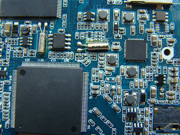
Improving yield requires control across the complete manufacturing chain.
Control Material Variation
PCB materials should be selected according to the required dimensional stability and electrical performance.
Material thickness, copper distribution, dielectric construction, and thermal behavior can all affect registration.
Optimize the Stackup
A carefully designed stackup reduces unnecessary complexity and makes via depth and lamination requirements easier to control.
The stackup should be reviewed before manufacturing to ensure that each via structure can be produced within the available process window.
Monitor Tool Condition
Drill wear should be tracked rather than relying solely on a fixed replacement schedule.
Tool condition can affect hole geometry, roughness, debris generation, and dimensional accuracy.
Control Lamination Parameters
Temperature, pressure, heating rate, cooling conditions, prepreg selection, and resin flow all influence multilayer dimensional stability.
Consistent lamination conditions help reduce layer movement and thickness variation.
Validate Plating Performance
Copper thickness and distribution should be verified at critical via structures.
Process monitoring can help identify plating variation before it develops into a larger production problem.
When Should You Use Blind and Buried Vias?
Blind and buried vias are particularly useful when PCB routing density is high and board size must be minimized.
They can be considered for:
- Smartphones and portable electronics
- High-density computing equipment
- Communication systems
- Medical electronics
- Automotive electronics
- Aerospace electronics
- Advanced industrial controls
- High-performance embedded systems
However, these structures should not be added simply because they are technically available.
If a conventional through-via design can meet the electrical, mechanical, and routing requirements, it may provide a simpler and more economical manufacturing solution.
The decision should balance:
Routing density + electrical requirements + board size + manufacturing capability + reliability + cost
Blind and Buried Via PCB Manufacturing Cost Factors
The additional manufacturing complexity generally makes blind and buried via PCBs more expensive than conventional through-hole multilayer boards.
Major cost drivers include:
- Additional drilling operations
- Laser drilling requirements
- Sequential lamination
- Advanced registration
- Additional plating processes
- Specialized inspection
- Higher material requirements
- Tighter manufacturing tolerances
- Increased process-control requirements
However, the higher fabrication cost may be justified when the design requires smaller board dimensions, higher routing density, or improved electrical performance.
For development-stage products, prototype production can be particularly useful for validating the stackup, via structure, drilling parameters, and registration strategy before moving into larger production volumes.
From Prototype to Volume Production
Complex blind and buried via structures should ideally be validated before full-scale manufacturing.
A prototype build can help engineers evaluate:
- Via geometry
- Layer registration
- Lamination behavior
- Copper plating
- Electrical continuity
- Board thickness
- Manufacturing yield
- Reliability performance
Once the design and process are validated, production can be scaled according to demand. For projects requiring coordinated component sourcing and assembly, an integrated turnkey PCB assembly workflow can simplify the transition from fabricated PCB to assembled electronic product.
For larger production programs, consistent process control becomes increasingly important. High-volume PCB assembly can support standardized production processes after the design and manufacturing parameters have been validated.
Key Takeaways
The major challenges of blind and buried via PCB manufacturing are closely related to dimensional accuracy and process consistency.
The most important areas include:
- Precise blind via depth control
- Accurate layer-to-layer registration
- Reliable microvia drilling
- Consistent copper plating
- Stable lamination and resin flow
- Multilayer thickness control
- Effective internal inspection
- Tight process and material control
Advanced technologies such as laser drilling, optical registration, controlled copper plating, and sequential lamination can significantly improve manufacturing capability.
At the same time, successful production begins with a manufacturable PCB design. Via geometry, stackup construction, material selection, and tolerance requirements should all be evaluated before fabrication.
Conclusion
A Blind and Buried Via PCB provides an effective solution for high-density electronic designs that require greater routing flexibility within a limited board area. However, its manufacturing process is significantly more demanding than conventional through-hole PCB fabrication.
Drilling depth, microvia formation, layer registration, copper plating, lamination, resin flow, and dimensional stability must all be carefully controlled. A small deviation at any stage can affect electrical connectivity, manufacturing yield, or long-term reliability.
For this reason, HDI PCB manufacturing and blind/buried via production require close coordination between PCB design engineers and manufacturing engineers.
By optimizing the stackup, selecting appropriate materials, controlling drilling and plating parameters, validating lamination behavior, and applying suitable inspection methods, manufacturers can achieve more consistent results and reduce production risks.
For complex PCB projects, working with a manufacturer capable of coordinating design review, fabrication, assembly, inspection, and production scaling can provide a more efficient path from prototype validation to reliable volume production.