How to Repair a Keyboard PCB: Keyboard PCB Repair, Troubleshooting & Rework Guide
The development of electronic technology has transformed nearly every modern product and application. From early computing systems to today’s compact smart devices, each generation of computers has evolved alongside advances in electronics, semiconductor technology, and PCB design. Printed circuit boards provide the electrical interconnections that allow processors, memory, interfaces, power circuits, and peripheral devices to operate as an integrated system.
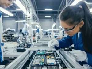
The keyboard is one of the most important human-machine input devices in a computer system. Although modern keyboards may appear relatively simple from the outside, their internal electronics can include a keyboard PCB, key-switch matrix, controller, LEDs, USB or wireless interface, and supporting components.
Like any electronic assembly, a keyboard PCB can develop faults caused by liquid spills, contamination, mechanical stress, corrosion, cracked solder joints, damaged traces, failed components, connector problems, or firmware and configuration issues. Even when the PCB is securely mounted inside the keyboard housing, damage can still occur over time.
Fortunately, many common keyboard PCB problems can be diagnosed and repaired when the damage is localized and the board remains structurally sound. This guide explains how to repair a keyboard PCB, covering diagnosis, trace repair, solder rework, component replacement, cleaning, testing, and preventive practices.
Repair vs. Replacement: Which Is Better?
Before starting PCB repair, determine whether repairing the keyboard PCB is technically and economically reasonable.
A localized problem such as contamination, a cracked solder joint, a damaged trace, or a failed discrete component may be practical to repair. In contrast, extensive carbonization, severe corrosion, widespread delamination, major mechanical damage, or damage to critical multilayer interconnections can make repair unreliable or uneconomical.
A simple decision framework is useful:
| Condition | Recommended Approach |
|---|---|
| Contamination or residue | Clean and inspect |
| Cracked solder joint | Re-solder |
| Localized damaged trace | Trace/jumper repair |
| Failed diode, resistor, capacitor, or connector | Component replacement |
| Lifted or damaged pad | Pad reconstruction or professional repair |
| Severe corrosion | Evaluate affected circuits before repair |
| Burned or carbonized PCB area | Repair only if structurally and electrically feasible |
| Extensive multilayer damage | Consider PCB or keyboard replacement |
Repair is generally worthwhile when the fault is clearly localized and the required repair can restore the original electrical and mechanical characteristics.
However, if a substantial section of the board is burned or internal multilayer connections are compromised, replacing the PCB or the entire keyboard may be more practical.
General Diagnostic Procedure Before Keyboard PCB Repair
Accurate diagnosis should always come before repair. Replacing components or soldering traces without first identifying the root cause can introduce additional faults.
A structured diagnostic process can reduce unnecessary rework and help determine whether the problem originates from the keyboard PCB, switch matrix, controller, connector, firmware, or another part of the keyboard.
1. Clearly Identify and Describe the Problem
Begin by documenting the symptoms.
Important questions include:
- Which keys are not working?
- Is an entire row or column of keys affected?
- Are only individual keys malfunctioning?
- Are the keyboard LEDs working?
- Is the USB or wireless connection stable?
- Is the keyboard detected by the computer?
- Was the keyboard exposed to liquid?
- Are there visible broken traces or damaged pads?
- Are there loose or cracked solder joints?
- Has the keyboard recently been modified or reassembled?
- Does the problem occur intermittently or continuously?
The pattern of failed keys can provide important clues. For example, multiple keys failing in the same matrix row or column may indicate a damaged matrix trace, diode, connector, or controller path rather than several independent switch failures.
2. Perform a Visual Inspection
Careful visual inspection is one of the simplest and most useful steps in PCB troubleshooting.
Disconnect the keyboard from its power source before inspecting the board. Under good lighting, examine the PCB for:
- Burn marks or discoloration
- Corrosion
- Liquid residue
- Cracked solder joints
- Lifted or damaged pads
- Broken traces
- Missing components
- Damaged connectors
- Loose wires
- Mechanical cracks
- Contaminated switch contacts
- Signs of overheating
A magnifying glass or inspection microscope can be particularly useful for fine-pitch components and narrow PCB traces.
For boards with visible liquid damage, inspect not only the obvious contaminated area but also nearby connectors, vias, component leads, and solder joints. Liquid can migrate underneath components and create leakage paths or corrosion that is not immediately visible.
3. Check Power and Connections
Before performing resistance or continuity measurements, make sure the keyboard is disconnected from USB power, batteries, or other power sources.
Check the physical connection between the keyboard PCB and its external interface. Depending on the design, this may include:
- USB connector
- USB-C connector
- Ribbon cable
- Wireless module
- Battery connector
- Daughterboard connector
- Internal cable harness
A damaged connector can produce symptoms that appear to be a PCB failure.
When appropriate, use a multimeter to check continuity between accessible points. However, a continuity beep alone does not automatically prove that a circuit is healthy. Components, capacitors, parallel paths, and semiconductor junctions can affect resistance measurements.
4. Check the Key Switch Matrix and Components
Most conventional keyboards use a row-and-column matrix rather than connecting every key directly to an individual controller input.
Depending on the keyboard architecture, individual keys may work together with:
- Mechanical or membrane switches
- Diodes
- Row traces
- Column traces
- Controller IC
- Pull-up or pull-down networks
- LEDs
- Communication circuitry
If a single key fails, inspect its switch, solder joints, diode, and associated traces.
If multiple keys in the same row or column fail, investigate the shared electrical path. This approach can significantly narrow down the defective area.
For mechanical keyboards, a failed switch can sometimes be replaced without replacing the entire PCB. If the switch itself is functioning but the key is not detected, the PCB trace, solder joint, diode, or controller path should be investigated.
5. Check Firmware and Configuration
Some programmable keyboards contain firmware that controls the key matrix, lighting, macros, communication interface, and other functions.
If the hardware appears intact but the keyboard behaves incorrectly, check:
- Firmware version
- Keyboard layout
- Matrix configuration
- Remapping settings
- USB configuration
- Wireless pairing
- Bootloader mode
- Custom firmware settings
Firmware problems should not automatically be interpreted as physical PCB damage.
If the manufacturer provides an official firmware recovery or update procedure, follow that procedure carefully. Do not interrupt power during firmware flashing unless the applicable procedure specifically permits it.
Common Methods for Repairing a Keyboard PCB
Once the fault has been identified, select a repair method that matches the type and severity of damage.
1. Clean Corrosion, Dirt, and Residue
Contamination is a common cause of keyboard problems, particularly after liquid spills or long-term exposure to dust and humidity.
Depending on the PCB materials and contamination involved, an appropriate electronics-grade cleaning agent may be used. Isopropyl alcohol (IPA) is commonly used for removing many residues, although the correct cleaning method depends on the contaminant and component materials.
A typical cleaning process includes:
- Disconnect the keyboard from all power sources.
- Remove loose dust and debris.
- Inspect the affected area under magnification.
- Apply an appropriate PCB-safe cleaning agent.
- Gently clean the contaminated area.
- Remove loosened residue.
- Allow the PCB to dry completely.
- Inspect again for corrosion or damaged traces.
- Test the circuit before final assembly.
Do not assume that cleaning alone has removed corrosion damage. If copper traces, component leads, vias, or pads have already corroded, additional PCB repair may be necessary.
2. Repair Broken PCB Traces
A broken trace can interrupt a row, column, power path, LED circuit, or communication signal.
For a localized open circuit, a suitable jumper wire can sometimes restore the electrical connection.
A typical trace repair procedure is:
- Identify both ends of the damaged trace.
- Verify the open circuit with a suitable measurement.
- Carefully remove solder mask from a small area of intact copper.
- Clean the exposed copper.
- Apply appropriate flux.
- Solder a suitable repair wire or conductor between the intact points.
- Secure the repaired wire if mechanical movement could stress the solder joints.
- Check continuity and isolation.
- Perform functional testing.
For very fine traces, conductive repair materials may be appropriate in some applications, but their electrical and mechanical performance should be considered carefully.
Copper foil or PCB repair tape can also be used for certain larger damaged areas, provided it is properly bonded and electrically connected.
The repair should restore the intended circuit without creating accidental connections to adjacent traces.
3. Re-Solder Cracked or Defective Joints
Cracked solder joints are another common source of intermittent keyboard faults.
Typical symptoms include:
- A key works only when pressed or flexed
- LEDs flicker
- USB connection intermittently disconnects
- The keyboard works after tapping or moving it
- A connector feels mechanically unstable
For a defective solder joint:
- Disconnect all power.
- Inspect the joint under magnification.
- Remove excess or degraded solder if necessary.
- Apply a suitable flux.
- Reheat the joint using a temperature-controlled soldering iron.
- Add an appropriate amount of solder.
- Allow the joint to cool without mechanical movement.
- Inspect the finished joint.
Excessive heat should be avoided because prolonged heating can lift pads, damage components, or weaken PCB materials.
4. Replace Failed Components
If testing confirms that a component has failed, replacement may be more appropriate than simply re-soldering it.
Potentially defective components include:
- Diodes
- Resistors
- Capacitors
- LEDs
- Voltage regulators
- Connectors
- Switches
- Crystals or oscillators
- Other discrete components
The replacement component should match the original part’s electrical and mechanical requirements. Do not select a replacement based only on physical appearance.
For polarized components such as diodes, electrolytic capacitors, and LEDs, correct orientation is essential.
5. Repair Damaged Pads
A damaged or lifted solder pad requires greater care than a simple trace repair.
If the pad is partially lifted but still electrically connected, avoid applying mechanical force that could worsen the damage. Depending on the application, the pad may be stabilized and repaired using an appropriate PCB repair technique.
If the pad is completely missing, a replacement repair pad or suitable copper structure may be required. The repaired pad must have adequate mechanical support and electrical connection.
Special attention is necessary when the pad connects to:
- Internal PCB layers
- A plated through-hole
- A via
- A high-current path
- A high-speed signal
Simply recreating the visible surface copper does not necessarily restore an internal multilayer connection.
For complex or high-density boards, professional PCB pad repair may be preferable.
How to Repair a Keyboard PCB Step by Step
For a localized fault, the overall process can be organized into the following workflow:
Step 1: Disconnect Power
Disconnect the USB cable and remove the battery if the keyboard contains one.
Step 2: Disassemble Carefully
Remove the keyboard housing and mechanical components without stressing the PCB, ribbon cables, connectors, or switch assemblies.
Step 3: Document the Original Configuration
Take photographs and note connector orientation, cable routing, screw positions, and component locations before disassembly.
Step 4: Inspect the PCB
Look for contamination, corrosion, broken traces, damaged pads, defective solder joints, and missing components.
Step 5: Identify the Electrical Fault
Use appropriate testing methods to determine whether the problem is associated with the key switch, diode, matrix trace, connector, controller, or another circuit.
Step 6: Perform the Repair
Depending on the diagnosis, clean the board, re-solder the joint, replace the component, repair the trace, or reconstruct the damaged pad.
Step 7: Inspect the Repair
Check for solder bridges, unintended connections, loose wires, excessive solder, and mechanical instability.
Step 8: Test Electrically
Verify continuity and isolation where appropriate. Avoid relying on a single measurement as proof that the entire circuit is healthy.
Step 9: Perform Functional Testing
Reconnect the keyboard and test individual keys, multiple-key combinations, LEDs, USB communication, wireless functions, and other applicable features.
Step 10: Reassemble the Keyboard
Once the repair passes functional testing, reinstall the PCB and mechanical components carefully.
Best Practices and Safety Precautions
Following good PCB rework practices helps prevent additional damage during keyboard repair.
Observe ESD Precautions
Electronic components can be sensitive to electrostatic discharge. Use appropriate ESD protection and work on a suitable grounded workstation when handling sensitive electronics.
Disconnect Power Before Repair
Never solder or perform resistance/continuity measurements on an energized keyboard PCB unless the specific measurement procedure is designed for live testing.
Use Temperature-Controlled Soldering Equipment
A temperature-controlled soldering iron provides better control than an uncontrolled high-temperature iron. Excessive heat can damage pads, traces, switches, connectors, and components.
Use Suitable Replacement Parts
Replacement components should meet the required electrical specifications, package dimensions, polarity, and mechanical requirements.
Avoid Excessive Mechanical Force
PCB substrates, pads, vias, connectors, and small components can be damaged easily. Do not bend or flex the board unnecessarily during troubleshooting.
Use Proper Inspection and Testing Tools
Useful tools may include:
- Digital multimeter
- Temperature-controlled soldering iron
- Soldering accessories
- Flux
- Magnifying glass or microscope
- ESD-safe tools
- PCB cleaning materials
- Fine repair wire
- Tweezers
- Suitable PCB repair materials
The exact tools required depend on the complexity of the keyboard PCB and the type of failure.
When Should You Stop Repairing a Keyboard PCB?
Not every PCB should be repaired.
Consider replacement when:
- A large section of the PCB is severely burned.
- The PCB substrate is extensively carbonized.
- Multiple internal layers are damaged.
- Major controller circuitry has failed and replacement parts are unavailable.
- Corrosion has affected a large portion of the board.
- Critical pads and vias have been destroyed.
- The repair cost approaches or exceeds the replacement cost.
- The repaired board cannot meet the required reliability level.
A successful repair is not simply a board that works once. The repaired PCB should provide adequate electrical, mechanical, and functional reliability for its intended use.
Repair vs. Professional PCB Manufacturing
For simple keyboard faults, local PCB repair can often restore functionality without replacing the entire board. However, when the board itself has extensive damage or the keyboard requires a replacement PCB, professional PCB manufacturing may be the more appropriate solution.
A replacement PCB may require:
- Original or reconstructed PCB design files
- Schematic information
- Gerber manufacturing files
- Drill files
- PCB stackup information
- Material specifications
- Copper thickness
- Surface finish
- Solder mask requirements
- Component placement data
- Electrical testing
- PCB assembly requirements
For custom replacement boards, working with an experienced manufacturer can help ensure that the replacement PCB matches the required mechanical dimensions and electrical characteristics.
Kingda can support customers with PCB manufacturing and related PCB production requirements, depending on the board design, material, layer structure, and manufacturing specifications.
Conclusion
Learning how to repair a keyboard PCB starts with accurate diagnosis rather than immediately replacing components or soldering wires. A systematic process—problem identification, visual inspection, electrical testing, matrix analysis, component inspection, targeted repair, and functional verification—can resolve many localized keyboard failures.
Common problems such as contamination, cracked solder joints, broken traces, damaged pads, defective switches, and failed discrete components may be repairable with the appropriate tools and techniques. However, severe corrosion, extensive burning, multilayer damage, or failed critical circuitry can make replacement more practical than repair.
For simple repairs, careful workmanship and proper testing are often sufficient. For complex or damaged boards, professional PCB manufacturing, PCB rework, or replacement PCB production may provide a more reliable long-term solution.
The key principle is simple: diagnose first, repair only what is necessary, and verify the complete keyboard PCB before final assembly.