PCB flatness is an important quality requirement throughout PCB Manufacturing and assembly. As electronic products become smaller, thinner, and more highly integrated, the dimensional stability and flatness of printed circuit boards have become increasingly critical.
During automated surface-mount assembly, excessive PCB Warpage can cause positioning errors, poor solder paste printing, component placement problems, and difficulties during reflow soldering. For through-hole components, excessive deformation may also interfere with insertion accuracy. In severe cases, warped boards can cause equipment stoppages or prevent the finished assembly from fitting properly into its enclosure.
For this reason, PCB warpage is not simply a cosmetic issue. It can directly affect manufacturing yield, assembly reliability, dimensional accuracy, and the overall performance of the finished electronic product.
1. What Is PCB Warpage?
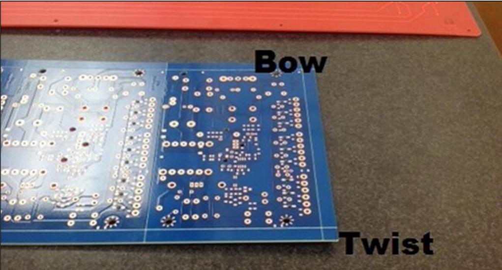
PCB Warpage refers to the deviation of a PCB from its intended flat or planar shape. Depending on the deformation pattern, a board may bend, twist, bow, or exhibit localized distortion.
PCB deformation can generally be classified into several forms:
- Bow: The board curves in one primary direction.
- Twist: Different areas of the board deform in different directions.
- Bending: The board develops a noticeable curved profile.
- Local deformation: A specific area becomes uneven because of localized stress or material variation.
The degree of deformation depends on board thickness, size, material construction, copper distribution, layer structure, processing conditions, and the thermal history of the PCB.
Industry requirements may specify maximum allowable deformation as a percentage of board dimensions. However, actual acceptance criteria can vary according to the applicable IPC standard, product type, assembly process, and customer requirements.
High-speed automated assembly lines often require tighter flatness control than general-purpose PCB applications.
2. Why PCB Warpage Matters During Assembly
Modern PCB Assembly equipment relies on accurate positioning and stable board geometry.
When a PCB is excessively warped, several problems may occur.
Automated Component Placement
Pick-and-place machines require the PCB surface to remain within an acceptable flatness range. Excessive deformation can change the reference position of component pads and interfere with accurate placement.
Solder Paste Printing
A warped PCB may not make uniform contact with the stencil. This can result in inconsistent solder paste deposition, insufficient solder volume, solder bridging, or other printing defects.
Reflow Soldering
During reflow, the PCB is exposed to elevated temperatures. Existing deformation may become more pronounced as the materials expand and soften.
This can contribute to:
- Open solder joints
- Insufficient solder contact
- Component displacement
- Uneven soldering
- Tombstoning in certain components
- Increased assembly defects
Mechanical Assembly
A warped PCB may also be difficult to install into:
- Enclosures
- Connectors
- Mechanical supports
- Card slots
- Backplanes
- Heat sinks
Therefore, controlling PCB Deformation is essential for both electrical and mechanical integration.
3. Why Does PCB Deformation Occur?
A PCB is a composite structure consisting of copper foil, resin, glass reinforcement, prepreg, core materials, solder mask, and other materials.
These materials do not necessarily have identical:
- Coefficients of thermal expansion
- Elastic modulus
- Moisture absorption
- Shrinkage characteristics
- Thermal conductivity
- Curing behavior
During PCB Manufacturing, the board is repeatedly exposed to heating, cooling, pressing, chemical processing, mechanical machining, and storage.
These processes can create or release internal stresses.
The major contributors to PCB Warpage include:
- Uneven copper distribution
- Differences in material properties
- Lamination-induced stress
- Thermal cycling
- Uneven resin curing
- Drilling and mechanical processing
- Surface finishing and plating
- Solder mask curing
- Reflow or hot-air leveling
- Improper storage and handling
4. Uneven Copper Distribution
One of the most common causes of PCB deformation is an imbalance in copper distribution.
Many PCB designs contain large copper areas for ground or power planes. If one side of the board contains substantially more copper than the opposite side, the two sides can respond differently during heating and cooling.
Copper and dielectric materials have different thermal and mechanical properties. As the board temperature changes, each material attempts to expand or contract according to its characteristics.
When the copper distribution is balanced, these forces can partially offset each other.
When the distribution is highly asymmetric, however, the resulting stress can cause the PCB to bow or twist.
For this reason, Copper Distribution should be considered during PCB layout.
If one layer contains a large solid copper area while the corresponding layer contains very little copper, designers may consider appropriate copper balancing techniques where electrically and thermally acceptable.
5. The Influence of PCB Layer Structure
Multilayer PCBs consist of multiple cores, prepreg layers, copper foils, and dielectric structures.
The overall stackup should be as mechanically balanced as possible.
An asymmetrical stackup can create different thermal expansion and contraction behavior on opposite sides of the board.
For example, if the dielectric thickness or copper content above and below the central plane is significantly different, the resulting stress distribution may cause the board to deform during lamination or subsequent thermal processing.
A well-balanced multilayer stackup should consider:
- Core thickness
- Prepreg thickness
- Copper thickness
- Copper distribution
- Number of layers
- Resin content
- Material properties
- Symmetry around the central plane
Proper stackup design is therefore one of the most effective ways to reduce deformation before manufacturing begins.
6. Thermal Expansion and PCB Materials
The choice of PCB Materials has a direct influence on dimensional stability.
Copper has a relatively low in-plane coefficient of thermal expansion compared with the Z-axis expansion of many resin systems.
For FR-4 and similar materials, the coefficient of thermal expansion changes significantly around the glass transition temperature (Tg).
Below Tg, the resin system is relatively rigid and its thermal expansion is comparatively controlled.
Above Tg, the resin becomes much more flexible and its expansion in the Z-axis increases significantly.
Therefore, repeated exposure to temperatures above Tg can produce considerable mechanical stress, especially when different materials are constrained within the same multilayer structure.
Material selection should therefore consider:
- Tg
- CTE
- Resin content
- Dimensional stability
- Moisture absorption
- Thermal decomposition characteristics
- Lamination compatibility
For demanding applications, selecting materials with appropriate thermal and mechanical properties can significantly improve dimensional stability.
7. PCB Lamination and Residual Stress
PCB Lamination is one of the most important manufacturing stages affecting board flatness.
During lamination, cores, prepregs, and copper foils are combined under controlled temperature and pressure.
The resin in the prepreg melts, flows, and cures. However, resin flow and curing are not always perfectly uniform throughout the entire panel.
Variations can result from:
- Temperature distribution
- Pressure distribution
- Heating and cooling rates
- Resin flow
- Copper pattern density
- Material thickness
- Pressing conditions
- Panel construction
As the laminate cools after curing, residual stresses can remain inside the board.
These stresses may not immediately produce severe deformation. However, later processes such as drilling, baking, plating, solder mask curing, or reflow can release or redistribute the internal stress.
This is one reason why a board that appears flat after lamination may become warped later in the manufacturing process.
8. The Effect of Drilling and Mechanical Processing
Mechanical processing can also influence PCB Deformation.
Drilling removes material and generates localized mechanical and thermal stress. Large numbers of holes, uneven hole distribution, or aggressive drilling conditions can contribute to stress imbalance.
Routing, milling, V-scoring, and other mechanical processes can also alter the structural stiffness of the panel.
V-scoring is particularly important because it intentionally reduces the remaining material thickness between individual boards and the production panel.
If the V-score depth is excessive or uneven, the remaining material may not provide sufficient mechanical support, increasing the risk of deformation during handling and assembly.
Therefore, panelization and mechanical processing should be considered as part of the overall PCB structural design.
9. Solder Mask and Baking Processes
Solder mask curing is another thermal process that can influence board flatness.
During curing, the solder mask undergoes chemical and physical changes. If the amount or distribution of solder mask differs significantly between the two sides of the PCB, additional stress may be introduced.
Baking processes can also cause deformation when internal stresses are released at elevated temperatures.
The risk can be higher for thin PCBs because their mechanical stiffness is lower.
For thin multilayer boards, manufacturers should carefully control:
- Baking temperature
- Baking time
- Board orientation
- Support method
- Cooling conditions
10. Hot Air Solder Leveling and Thermal Shock
Hot Air Solder Leveling (HASL) exposes the PCB to relatively high temperatures for a short period.
The board is rapidly heated and then cooled during the process.
This thermal cycle can generate temporary and residual stresses, especially when the board contains:
- Asymmetric copper patterns
- Different material structures
- Thin dielectric layers
- Large copper areas
- Uneven layer construction
Rapid cooling immediately after high-temperature processing can further increase thermal stress.
Therefore, controlled cooling and proper board support are important for minimizing PCB Warpage.
For sensitive board constructions, gradual cooling under controlled conditions may be preferable to an abrupt temperature transition.
11. Storage and Handling
Not all PCB deformation is generated during fabrication.
Improper storage and handling can also cause mechanical deformation.
For example, boards that are stored vertically without adequate support may gradually bend under their own weight.
Improper stacking can also introduce localized pressure.
The risk becomes greater for:
- Large-format PCBs
- Thin PCBs
- Flexible or rigid-flex structures
- Heavy-copper boards
- Large multilayer boards
Proper storage should maintain adequate support and avoid excessive mechanical loading.
Boards should also be protected from uncontrolled moisture and temperature changes.
12. Preventing PCB Warpage Through Engineering Design
Preventing PCB Warpage should begin during engineering design rather than after manufacturing problems appear.
12.1 Use a Symmetrical Stackup
The layer construction above and below the central plane should be as symmetrical as practical.
Prepreg thickness, core thickness, and copper distribution should be evaluated together.
12.2 Balance Copper Distribution
Try to maintain a reasonable copper balance between opposing layers.
If one layer requires a large copper plane, an appropriate balancing pattern may be considered on the opposite side where it does not interfere with electrical performance.
12.3 Control Board Thickness
Very thin PCBs are more susceptible to mechanical deformation.
If a thin board is required by the product design, additional attention should be paid to stackup symmetry, material selection, panelization, and assembly support.
12.4 Optimize Panelization
Panel design should provide adequate mechanical support during manufacturing.
V-score depth, routing width, breakaway structures, and board orientation should all be optimized according to board thickness and geometry.
12.5 Select Appropriate Materials
Choosing suitable PCB Materials can reduce thermal and mechanical stress.
For demanding applications, manufacturers should evaluate Tg, CTE, resin content, dimensional stability, and moisture resistance.
13. Controlling Warpage During PCB Manufacturing
In addition to design optimization, manufacturers should establish appropriate process controls.
Important control points include:
- Incoming material inspection
- Material conditioning and baking
- Lamination temperature and pressure
- Resin flow control
- Cooling rate
- Drilling parameters
- Plating process
- Copper distribution
- Solder mask curing
- Surface finishing
- Panel handling
- Final flatness inspection
Each stage can influence the final board shape.
Consequently, PCB Manufacturing should be managed as a continuous process rather than treating warpage as an isolated final-inspection problem.
14. Measuring PCB Flatness
A reliable flatness measurement method is necessary to determine whether the finished PCB meets the required specification.
Depending on the application, manufacturers may use:
- Precision flatness tables
- Mechanical gauges
- Optical measurement systems
- Automated dimensional inspection
- Dedicated warpage measurement equipment
Measurement conditions should be standardized because temperature, humidity, board orientation, support method, and measurement location can influence the result.
For high-volume production, statistical process control can also be used to monitor warpage trends and identify process drift before it results in significant production problems.
15. Corrective Methods for Warped PCBs
When deformation occurs, corrective treatment may sometimes be possible, depending on the board construction and severity of the deformation.
Controlled heating combined with mechanical flattening can reduce certain types of warpage.
However, corrective processing should be carefully validated because excessive temperature or pressure can cause:
- Delamination
- Resin degradation
- Pad damage
- Solder mask cracking
- Dimensional instability
- Reliability problems
Therefore, prevention through material selection, stackup optimization, and process control is generally preferable to attempting to repair severely warped boards after fabrication.
16. Kingda’s Approach to PCB Warpage Control
At Kingda, controlling PCB Warpage is approached through the combined management of design, materials, stackup, lamination, fabrication, and inspection.
For multilayer and thin-board applications, key factors such as copper balance, stackup symmetry, material characteristics, lamination conditions, mechanical processing, and thermal exposure should be evaluated together.
Kingda can also work with customers during the engineering stage to identify structures that may have elevated deformation risk.
By incorporating manufacturability considerations into the PCB design process, potential warpage problems can be addressed before mass production.
The goal is not simply to produce a board that meets the dimensional drawing, but to maintain consistent flatness throughout manufacturing and subsequent PCB Assembly.
17. Key Takeaways
PCB Warpage is a complex problem caused by the interaction of materials, board structure, thermal stress, copper distribution, mechanical processing, and manufacturing conditions.
The most important factors include:
- Copper Distribution should be reasonably balanced between layers.
- The multilayer stackup should be mechanically symmetrical whenever possible.
- PCB Materials should be selected according to thermal and dimensional requirements.
- PCB Lamination must provide consistent temperature, pressure, resin flow, and cooling.
- Mechanical processes such as drilling, routing, and V-scoring can influence board deformation.
- Thermal processes such as solder mask curing and surface finishing can release residual stress.
- Thin PCBs require tighter control because they have lower mechanical stiffness.
- Proper storage and handling are necessary to prevent mechanical deformation.
- Flatness should be monitored throughout PCB Manufacturing, not only during final inspection.
- Early design-for-manufacturing analysis can significantly reduce the risk of warpage.
Conclusion
As PCB designs become thinner, larger, denser, and more complex, controlling PCB Deformation is becoming increasingly important.
PCB warpage does not originate from a single manufacturing step. Instead, it is usually the result of interactions among material properties, copper distribution, layer construction, lamination, thermal processing, mechanical machining, and handling.
For this reason, effective warpage control requires a systematic approach that begins with engineering design and continues through PCB Manufacturing and PCB Assembly.
By optimizing stackup symmetry, balancing copper distribution, selecting suitable PCB Materials, controlling thermal and mechanical processes, and implementing reliable flatness inspection, manufacturers can significantly improve PCB dimensional stability and assembly performance.
Kingda is committed to integrating design-for-manufacturing principles with controlled fabrication processes to help customers achieve stable, reliable, and production-ready PCB solutions.