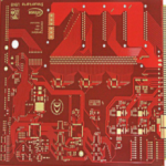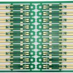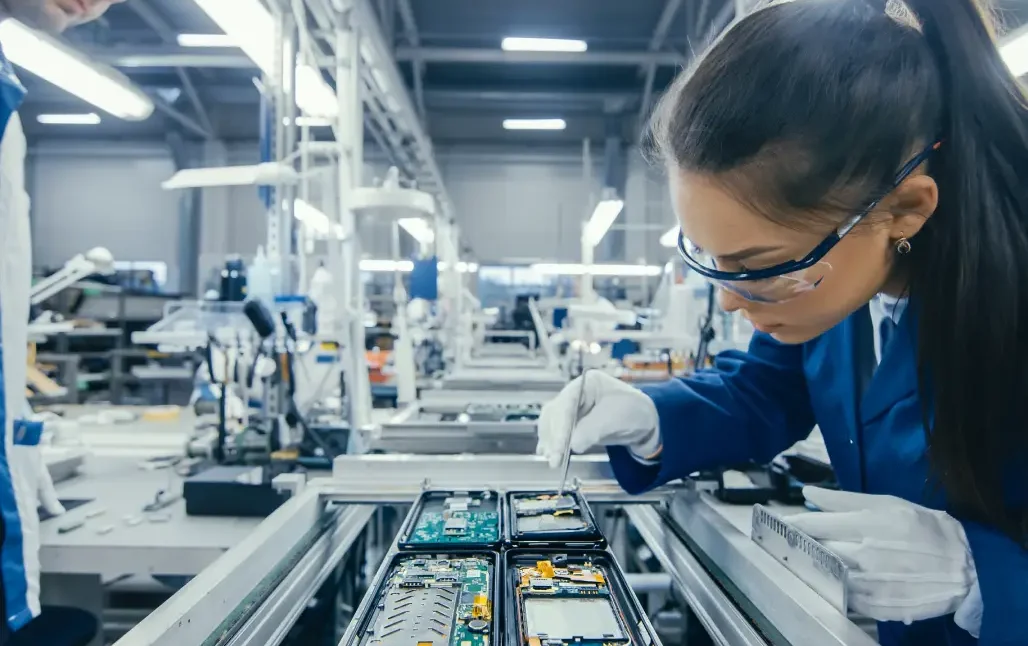
How to Repair a Damaged PCB: PCB Repair, Pad Repair & Trace Repair Guide
Printed circuit boards (PCBs) are fundamental components of almost every modern electronic product. From consumer electronics and automotive systems to industrial controls, medical equipment, telecommunications, and power electronics, PCBs provide the electrical and mechanical foundation for connecting components and enabling electronic functions.
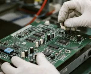
As electronic products become increasingly compact and multifunctional, PCB structures have also become more sophisticated. Modern boards may contain multiple copper layers, fine-pitch components, microvias, blind and buried vias, high-density interconnects, and highly optimized signal and power networks.
Although PCBs are designed for long-term operation, they can still be damaged by mechanical stress, excessive heat, electrical overstress, moisture, contamination, corrosion, improper handling, or component failure. Common damage includes cracked substrates, burned areas, broken traces, lifted pads, damaged vias, and failed components.
In some situations, a damaged board can be restored through professional PCB Repair. However, not every damaged PCB should be repaired. The feasibility of repair depends on the board construction, damage location, electrical requirements, mechanical integrity, safety requirements, and the ability to verify the repaired structure.
This guide explains How to Repair a Damaged PCB, covering PCB inspection, cleaning, substrate repair, trace repair, pad repair, component replacement, testing, troubleshooting, and the situations in which PCB replacement may be more appropriate.
What Is PCB Repair?
PCB Repair is the process of restoring a damaged printed circuit board so that its electrical connections, mechanical structure, and functional performance can meet the applicable requirements.
Depending on the type of damage, repair may involve:
- Replacing damaged components
- Repairing broken PCB traces
- Reconstructing lifted or missing pads
- Repairing damaged vias
- Restoring electrical connections
- Reinforcing localized substrate damage
- Removing corrosion or contamination
- Reworking defective solder joints
- Performing electrical and functional testing
The repair process should always begin with diagnosis rather than immediately applying solder or replacing components.
A visible defect does not necessarily represent the complete failure mechanism. For example, a burned component may be the result of an upstream power problem, while a lifted pad may have been caused by excessive rework temperature or mechanical stress.
Therefore, identifying the root cause is an important part of a reliable PCB Repair Process.
Common Causes of Damaged PCBs
Understanding why a PCB failed can help determine whether it can be repaired and how the repair should be performed.
Mechanical Damage
Mechanical stress is one of the most common causes of physical PCB damage.
Examples include:
- Dropping the equipment
- Excessive bending or twisting
- Impact during transportation
- Excessive connector insertion force
- Incorrect installation
- Vibration and mechanical shock
- Improper handling during assembly or maintenance
Mechanical damage can result in cracked laminate, broken traces, lifted pads, damaged vias, and fractured solder joints.
Excessive Heat
High temperatures can affect both PCB materials and electronic components.
Potential causes include:
- Overloaded power components
- Insufficient heat dissipation
- Poor airflow
- Excessive soldering temperature
- Incorrect rework conditions
- Repeated thermal cycling
Severe thermal damage may cause delamination, discoloration, carbonization, solder-joint degradation, or permanent damage to components.
Electrical Overstress
Electrical failures can produce severe localized PCB damage.
Typical causes include:
- Overvoltage
- Overcurrent
- Short circuits
- Voltage surges
- Electrostatic discharge
- Incorrect power connections
- Transient electrical events
Excessive current can generate enough heat to burn PCB traces or damage copper features.
Moisture and Contamination
Moisture, dust, flux residues, chemicals, and other contaminants can reduce PCB reliability.
Contamination can contribute to:
- Corrosion
- Leakage current
- Reduced insulation resistance
- Electrochemical migration
- Poor solderability
- Intermittent electrical failures
Improper Storage and Transportation
PCB damage can occur before a board is even installed in a product.
Excessive stacking, poor packaging, uncontrolled humidity, electrostatic discharge, and physical impact can all affect PCB condition.
Proper ESD protection, packaging, handling, and environmental control are therefore important throughout the PCB lifecycle.
How to Repair a Damaged PCB: Step-by-Step Process
A professional PCB Board Repair workflow should be systematic and controlled. The exact repair procedure depends on the type and severity of damage.
The general process includes:
- Preparing the repair workstation
- Inspecting and diagnosing the PCB
- Removing damaged components
- Cleaning the board
- Repairing the substrate when appropriate
- Repairing broken traces and vias
- Repairing lifted or missing pads
- Replacing damaged components
- Performing electrical and functional tests
- Documenting and validating the repair
1. Prepare a PCB Repair Workstation
A controlled repair workstation is essential for reliable PCB Repair.
The workspace should preferably include:
- ESD-safe workbench
- ESD wrist strap and grounding system
- Temperature-controlled soldering iron
- Hot-air rework station
- Digital multimeter
- Microscope or magnification system
- Precision tweezers
- Solder wick
- Desoldering tools
- Appropriate solder and flux
- PCB-safe cleaning agents
- Repair wire or copper foil
- Suitable PCB repair adhesive
- Test fixtures when required
The technician should also have access to the original PCB documentation whenever possible, including:
- Schematic
- PCB layout
- BOM
- Assembly drawings
- Component specifications
- Manufacturing drawings
- Test requirements
Before working on the board, ensure that the equipment is disconnected from power and that stored electrical energy has been safely discharged according to the equipment’s safety procedures.
2. Inspect and Diagnose the Damaged PCB
Inspection is one of the most important stages of PCB Troubleshooting.
Begin with a visual inspection under magnification.
Look for:
- Cracked PCB substrate
- Burn marks
- Broken traces
- Lifted pads
- Missing pads
- Damaged vias
- Corrosion
- Delamination
- Damaged connectors
- Cracked components
- Loose components
- Defective solder joints
The technician should determine whether the damage is limited to the surface or extends into the internal PCB structure.
Electrical Diagnosis
Electrical measurements can provide additional information.
Depending on the circuit, measurements may include:
- Resistance
- Continuity
- Isolation
- Voltage
- Current
- Power-rail measurements
- Signal measurements
However, continuity or low-resistance readings should not automatically be interpreted as a short circuit. Capacitors, semiconductor devices, parallel paths, and other circuit elements can affect in-circuit measurements.
For complex boards, compare the damaged PCB with its original design files or an undamaged reference board whenever possible.
3. Remove Damaged Components Carefully
If a failed component must be replaced, it should be removed using an appropriate rework technique.
Possible methods include:
- Soldering iron rework
- Hot-air rework
- Desoldering equipment
- Local preheating
- Specialized BGA rework equipment
The primary objective is to remove the defective component without causing additional damage to surrounding pads, traces, vias, or the laminate.
Fine-pitch components and BGA packages require particular attention because excessive heat or mechanical force can damage nearby structures.
After removal, inspect the exposed pads before installing the replacement component.
4. Clean the PCB Before Repair
Cleaning helps remove contaminants and makes the damaged area easier to inspect.
For many electronic assemblies, isopropyl alcohol (IPA) can be used to remove certain flux residues and surface contamination when it is compatible with the materials and components involved.
A typical cleaning procedure is:
- Apply an appropriate PCB-safe cleaning agent.
- Remove contamination carefully.
- Inspect the affected area under magnification.
- Allow the board to dry completely.
- Verify that no harmful residue remains.
Severe corrosion should not simply be cleaned and ignored. If copper conductors, component leads, or plated structures have been substantially degraded, they may need to be repaired or replaced.
5. Repair a Cracked or Damaged PCB Substrate
Repairing physical PCB damage requires careful evaluation.
A localized crack in a simple single-sided or double-sided PCB may sometimes be stabilized and electrically reconstructed if the surrounding material remains structurally sound.
Possible repair methods include:
- Stabilizing the cracked area
- Restoring broken copper conductors
- Applying suitable PCB repair adhesive
- Reinforcing the damaged section
- Reconnecting broken electrical paths
However, multilayer PCBs require much more extensive analysis.
A visible crack may extend through:
- Internal copper layers
- Power planes
- Ground planes
- Plated through-hole barrels
- Vias
- Dielectric layers
- Buried structures
Therefore, reconnecting only the visible surface traces does not prove that the entire multilayer structure has been restored.
If the board is severely cracked, delaminated, burned, or structurally compromised, replacement may be more appropriate than repair.
6. Repair Broken PCB Traces
PCB Trace Repair is a common repair technique for localized circuit damage.
To repair a broken trace, the damaged area is normally prepared by carefully removing enough solder mask to expose sound copper on both sides of the break.
Depending on the application, the connection can be restored using:
- Fine repair wire
- Copper foil
- Copper tape designed for PCB repair
- Appropriate soldering techniques
- Specialized PCB repair materials
The repair method must consider the electrical characteristics of the original trace.
Important factors include:
- Current capacity
- Voltage
- Trace width
- Signal frequency
- Controlled impedance
- Differential-pair requirements
- Mechanical stress
- Environmental conditions
Avoid Uncontrolled Solder Bridging
Simply filling a large gap with solder is not necessarily a reliable trace-repair method.
For low-current, low-frequency connections, solder-based reconstruction may sometimes be practical. However, high-current, high-speed, RF, or impedance-controlled traces require a repair method that preserves the required electrical characteristics as closely as possible.
After repairing the trace, verify:
- Electrical continuity
- Isolation from adjacent traces
- Mechanical stability
- Functional performance
7. Repair Lifted or Missing PCB Pads
PCB Pad Repair is another common form of board-level rework.
Pads can become damaged because of:
- Excessive soldering temperature
- Repeated component removal
- Mechanical stress
- Excessive insertion force
- Poor laminate adhesion
- Physical impact
Repairing a Lifted Pad
If the pad is partially attached and the underlying connection remains usable, it may sometimes be carefully repositioned and mechanically reinforced.
Suitable adhesive or repair material can be used where appropriate, but it must not contaminate the solderable area.
Repairing a Missing Pad
If a pad has been completely removed, a replacement pad can sometimes be reconstructed using suitable copper foil, copper tape, or a dedicated PCB pad-repair system.
The replacement pad must:
- Match the original location
- Establish the correct electrical connection
- Remain mechanically stable
- Maintain appropriate electrical isolation
- Provide a suitable solderable surface
For pads connected to internal layers through vias or plated structures, surface-level pad reconstruction may not be sufficient. The internal electrical path must also be considered.
This is particularly important for multilayer PCBs, HDI boards, and fine-pitch components.
8. Repair Damaged PCB Vias
Vias provide electrical connections between different PCB layers, making via damage more complicated than ordinary surface trace damage.
Possible via defects include:
- Cracked via barrels
- Damaged via pads
- Broken connections
- Corrosion
- Mechanical fractures
- Damage around the via
A repair wire may sometimes be used to restore an accessible electrical connection, but the repair must follow the original circuit topology.
Blind vias, buried vias, and microvias are more difficult to repair because their internal structures may not be directly accessible.
For advanced multilayer or HDI boards, professional analysis may be necessary before attempting a repair.
9. Replace Damaged PCB Components
Once damaged PCB structures have been repaired, defective components can be replaced.
Before installing a replacement, verify:
- Part number
- Package type
- Electrical specifications
- Pin configuration
- Orientation
- Polarity
- Temperature rating
- Component compatibility
Replacing a failed component without identifying why it failed can lead to repeated failures.
For example, if a power MOSFET fails because of excessive voltage, replacing the MOSFET alone may not solve the problem. The associated gate-drive circuit, power supply, protection components, and load should also be evaluated.
10. Perform PCB Rework Testing and Validation
Testing is the final critical stage of the PCB Repair Process.
A repaired board should be evaluated against the applicable original design and functional requirements.
Visual Inspection
Inspect:
- Repaired traces
- Reconstructed pads
- Repair wires
- Solder joints
- Vias
- Component orientation
- Flux residues
- Mechanical reinforcement
Electrical Testing
Depending on the application, testing may include:
- Continuity testing
- Isolation testing
- Resistance measurements
- Power-rail verification
- Insulation testing where applicable
- Signal measurements
Functional Testing
Functional testing determines whether the repaired PCB performs its intended functions.
Testing may include:
- Power-up verification
- Communication testing
- Digital I/O testing
- Analog signal testing
- Sensor testing
- Load testing
- Firmware verification
- Interface testing
Thermal Testing
If the original failure was related to excessive heat, thermal behavior should also be evaluated.
Thermal imaging, temperature measurements, or controlled load testing can help determine whether the repaired board operates within acceptable thermal conditions.
A PCB that passes continuity testing is not necessarily a reliable repaired PCB. Electrical, mechanical, thermal, and functional performance should be considered together.
PCB Repair vs. PCB Replacement
Repairing a PCB can be practical for localized damage, but replacement may be more appropriate for severe structural damage.
| Damage Type | Repair Feasibility | Typical Consideration |
|---|---|---|
| Single failed component | High | Replace and test the component |
| Localized broken trace | High | Reconstruct electrical connection |
| Lifted pad | Often feasible | Depends on pad and internal connection |
| Missing pad | Often feasible | Requires proper pad reconstruction |
| Damaged accessible via | Application-dependent | Verify layer-to-layer connectivity |
| Cracked simple PCB | Application-dependent | Check mechanical integrity |
| Severe multilayer crack | Difficult | Internal damage may be inaccessible |
| Extensive charring | Low | Material and insulation may be compromised |
| Severe delamination | Low | Replacement may be more reliable |
| High-voltage insulation damage | Requires strict evaluation | Safety and insulation integrity are critical |
| Safety-critical PCB damage | Highly controlled | Follow applicable repair requirements |
The key question is not simply whether the board can physically be repaired. The more important question is whether the repaired PCB can reliably meet the required electrical, mechanical, thermal, and safety specifications.
Best Practices for Reliable PCB Repair
Following established repair practices can improve the quality and repeatability of PCB Repair.
Use ESD Protection
Sensitive semiconductor devices can be damaged by electrostatic discharge without visible physical evidence. ESD-safe tools and grounding practices should therefore be used.
Control Rework Temperature
Excessive heat can damage PCB pads, laminate, solder joints, and components.
Use controlled heating and appropriate thermal profiles whenever possible.
Work Under Magnification
Modern PCBs often contain very small pads, traces, vias, and component packages. Magnification improves inspection accuracy and helps prevent accidental damage.
Use Original PCB Documentation
The original schematic, PCB layout, BOM, and manufacturing data can significantly improve the accuracy of diagnosis and repair.
Verify Before Applying Power
Before powering a repaired board, inspect for:
- Short circuits
- Solder bridges
- Incorrect component orientation
- Incorrect repair wires
- Open connections
- Damaged insulation
Where appropriate, use a current-limited power source during initial startup to reduce the risk of additional damage.
Document Every Repair
Professional repair operations should document:
- Original failure
- Damaged locations
- Components replaced
- Trace repairs
- Pad repairs
- Repair materials
- Test results
- Final inspection results
Good documentation improves traceability and simplifies future troubleshooting.
When Should a Damaged PCB Be Replaced?
Not every PCB should be repaired.
Replacement should be seriously considered when:
- The laminate is extensively burned or carbonized
- Multiple internal layers are damaged
- The PCB has severe delamination
- High-voltage insulation has been compromised
- Critical internal connections cannot be verified
- Mechanical integrity cannot be restored
- The repair cannot satisfy reliability requirements
- The original failure mechanism cannot be identified
- Repair costs approach or exceed replacement costs
For medical, automotive, aerospace, high-voltage, high-power, and other safety-critical applications, repair decisions should follow applicable engineering, quality, and regulatory requirements.
How Kingda Can Support PCB Manufacturing and Replacement
Professional PCB Manufacturing can provide a practical solution when a damaged board is beyond economical or reliable repair.
Kingda can support customers with PCB manufacturing requirements based on the specified board structure, dimensions, materials, layer count, copper requirements, surface finish, and other project specifications.
For replacement PCB projects, customers should provide complete and accurate manufacturing information whenever available, such as:
- Gerber files
- NC drill files
- BOM
- Pick-and-place data
- Assembly drawings
- PCB specifications
- Stackup information
- Special manufacturing requirements
For boards requiring assembly, testing, or other production services, the manufacturing process should be coordinated with the specific electrical and mechanical requirements of the final product.
The appropriate solution—repair, refurbishment, or complete PCB replacement—should ultimately be determined according to the board’s construction, damage severity, application requirements, reliability expectations, and total cost.
Conclusion
Learning How to Repair a Damaged PCB requires much more than replacing a failed component or reconnecting a broken trace. A PCB is a complex combination of copper conductors, dielectric materials, vias, pads, solder joints, and electronic components. Damage that appears minor on the surface may extend into internal layers or affect the overall mechanical and electrical integrity of the board.
A reliable PCB Repair Process should therefore begin with careful inspection and root-cause diagnosis. The repair may then involve component removal, cleaning, substrate stabilization, PCB Trace Repair, PCB Pad Repair, via reconstruction, component replacement, and comprehensive electrical and functional testing.
Localized damage can often be repaired when the underlying PCB structure remains sound and the repair can be properly verified. However, severely cracked, burned, delaminated, or internally damaged boards may be better candidates for replacement.
For engineers and manufacturers, the most important objective is not simply to make a damaged PCB work again temporarily. The goal is to restore the board to a condition that meets the required electrical performance, mechanical integrity, thermal behavior, safety, and reliability requirements.
By applying controlled repair procedures, using appropriate tools and materials, documenting the work, and performing thorough validation, companies can make informed decisions about whether to repair or replace a damaged PCB.
SEO Keywords
PCB Repair, How to Repair a Damaged PCB, PCB Board Repair, PCB Trace Repair, PCB Pad Repair, Damaged PCB, PCB Repair Process, PCB Via Repair, PCB Troubleshooting, PCB Manufacturing
SEO Title
How to Repair a Damaged PCB: PCB Repair, Pad & Trace Guide
Meta Title
How to Repair a Damaged PCB: PCB Repair Guide | Kingda
Meta Description
Learn how to repair a damaged PCB, including PCB inspection, cleaning, trace repair, pad repair, via repair, component replacement, testing, troubleshooting, and PCB replacement.
URL Slug
/how-to-repair-damaged-pcb-repair-pad-trace-guide/
PCB Keywords
PCB Repair, Damaged PCB, PCB Board Repair, PCB Trace Repair, PCB Pad Repair, PCB Repair Process, PCB Via Repair, PCB Troubleshooting, PCB Testing, PCB Manufacturing