PV Microinverter PCB: Design, Manufacturing, and Reliability Guide
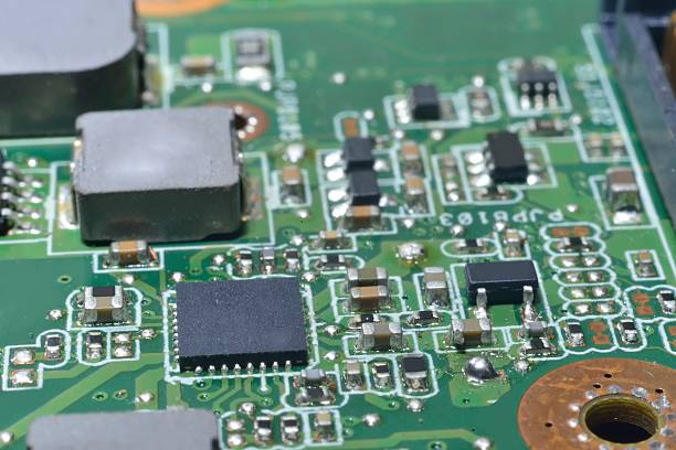
In a distributed photovoltaic (PV) system, the PV microinverter PCB is a critical electronic platform responsible for power conversion, control, monitoring, protection, and communication. Unlike a conventional centralized inverter architecture, a microinverter is typically associated with an individual PV module or a small number of modules, allowing power conversion to be performed closer to the solar panel.
This architecture places demanding requirements on the PCB. The board must handle switching currents and voltages, support high-frequency power electronics, dissipate heat efficiently, maintain electrical isolation where required, and remain reliable under outdoor temperature cycling, humidity, vibration, and other environmental stresses.
For solar equipment manufacturers, selecting the right solar inverter PCB manufacturing partner is therefore not simply a matter of producing a circuit board. PCB material selection, stackup design, copper distribution, thermal management, insulation, manufacturing tolerances, inspection, and electrical testing all contribute to the final reliability of the microinverter.
1. What Is a PV Microinverter PCB?
A PV microinverter PCB is a printed circuit board used inside a photovoltaic microinverter to integrate power conversion, sensing, control, protection, and communication functions.
The exact architecture varies according to the inverter topology and product requirements, but a typical microinverter PCB may include several functional areas:
Power Conversion Circuit
The power conversion section handles the primary energy-conversion process between the PV module’s DC output and the inverter’s AC output.
Depending on the topology, the circuit may contain MOSFETs, IGBTs, power diodes, inductors, transformers, capacitors, gate drivers, and other power-management components.
PCB layout is particularly important in this area because high-current loops and high-frequency switching nodes can generate voltage overshoot, electromagnetic interference (EMI), and additional losses if the layout is poorly optimized.
Sensing and Monitoring Circuit
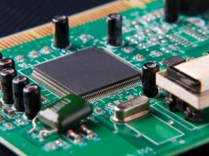
Voltage, current, temperature, and other operating parameters must be monitored to support control and protection functions.
Current-sensing circuits can measure PV input or output current, while voltage-sensing networks monitor electrical conditions. Temperature sensors may be positioned near power semiconductor devices, magnetic components, or other thermally sensitive areas.
Accurate sensing depends on both circuit design and PCB layout. Sensitive measurement traces should be appropriately separated from high-current and high-dv/dt switching paths to reduce noise coupling.
Control and Gate-Drive Circuit
A microcontroller, digital signal processor, or dedicated control device manages inverter operation according to the system architecture.
The control section may execute functions such as:
- Maximum power point tracking (MPPT)
- PWM generation
- Voltage and current regulation
- Grid synchronization
- Fault detection
- Thermal management
- Communication
- Protection control
Gate-drive circuits must be carefully designed because they directly influence the switching behavior of power semiconductor devices.
For complex products, professional PCB design and layout engineering can help optimize component placement, current loops, grounding, thermal paths, creepage, clearance, and signal integrity.
Protection Circuit
Protection functions are essential for photovoltaic power electronics.
Depending on the product architecture, protection may include:
- Overvoltage protection
- Overcurrent protection
- Overtemperature protection
- Short-circuit protection
- Surge protection
- Reverse-polarity protection
- Ground-fault or insulation monitoring
- Grid abnormality detection
- Anti-islanding protection
Anti-islanding functionality is particularly important in grid-connected PV systems. The specific implementation and applicable requirements depend on the inverter design and relevant regional standards.
Communication Interface
Modern microinverters increasingly support monitoring and communications.
The PCB may include interfaces for wired or wireless communication, allowing operating information, fault conditions, energy production data, and diagnostic information to be transmitted to a monitoring system.
2. Key PCB Requirements for Solar Microinverters
A photovoltaic microinverter operates in a significantly different environment from many indoor consumer electronics products.
The PCB must simultaneously satisfy electrical, thermal, mechanical, and environmental requirements.
High Electrical Stress
Power conversion circuits generate high currents and fast switching transitions. The PCB must therefore provide suitable conductor cross-sections, copper thickness, insulation distances, and thermal paths.
High-current traces should be designed to control temperature rise while minimizing unnecessary resistance and parasitic inductance.
Thermal Reliability
Heat is generated by switching devices, magnetic components, rectifiers, resistive elements, and other power components.
Poor thermal design can increase component temperature, accelerate aging, and reduce long-term reliability.
Thermal vias, copper planes, heat-spreading areas, appropriate component placement, and interfaces to heatsinks or enclosures may all contribute to thermal management.
Outdoor Environmental Exposure
Microinverters are commonly installed close to PV modules, where equipment can experience substantial temperature variation and humidity.
Depending on the installation environment, the PCB assembly may need protection against:
- Moisture
- Condensation
- Temperature cycling
- Dust
- Corrosive contaminants
- Mechanical vibration
- Electrical transients
PCB material, solder mask, surface finish, component selection, enclosure design, and conformal coating strategy should be considered together rather than independently.
3. PCB Material Selection for Photovoltaic Applications
Material selection has a direct effect on the reliability and manufacturability of a photovoltaic PCB.
Standard FR-4 can be suitable for many applications, but the appropriate laminate depends on temperature, electrical stress, layer count, signal requirements, mechanical construction, and expected service life.
High-Tg FR-4
High-Tg FR-4 materials can provide improved thermal stability compared with standard FR-4 formulations.
They may be considered when the PCB is subjected to elevated operating temperatures or repeated thermal cycling.
Important material parameters can include:
- Glass transition temperature (Tg)
- Decomposition temperature (Td)
- Z-axis CTE
- Thermal conductivity
- Moisture absorption
- Dielectric properties
High-Performance Materials
Certain microinverter designs may require specialized laminate systems based on electrical, thermal, or mechanical requirements.
For example, high-speed control or communication sections may require greater attention to dielectric properties, while power sections may place greater emphasis on thermal and electrical insulation performance.
Material selection should therefore be based on the actual operating conditions rather than simply selecting the material with the highest advertised temperature rating.
4. PCB Stackup and Layout Considerations
The PCB stackup has a major influence on both electrical and mechanical performance.
A well-designed multilayer board can provide dedicated power and ground structures, improve routing density, reduce loop areas, and help control electromagnetic emissions.
A typical design process should consider:
- Power and control circuit zoning
- High-current loop minimization
- Switching-node area reduction
- Ground and return-current paths
- Signal and power separation
- Thermal distribution
- Creepage and clearance
- Component accessibility
- Manufacturing constraints
Power switching loops should be kept compact to reduce parasitic inductance. Sensitive analog and control circuits should be positioned away from high-noise switching nodes wherever practical.
For higher-density designs, a carefully engineered multilayer PCB manufacturing process becomes increasingly important.
5. High-Current Copper Design for Solar Inverter PCBs
Copper thickness is an important factor in high-power PCB design, but simply increasing copper thickness does not automatically solve thermal or current-capacity problems.
The design must consider:
- Continuous current
- Peak current
- Trace width
- Copper thickness
- Temperature rise
- Layer configuration
- Via current distribution
- Copper plane area
- Heat dissipation
- Component terminal design
For high-current connections, wide copper areas and multiple vias may be used to distribute current and heat.
Where very high current density is required, designers may also consider heavy-copper PCB structures or other power-interconnect technologies.
The final copper configuration should be verified against the electrical and thermal requirements of the actual inverter rather than relying on a generic trace-width rule.
6. Thermal Management of a PV Microinverter PCB
Thermal management is one of the most important aspects of microinverter PCB engineering.
The power semiconductor devices are often among the most significant heat sources. If heat cannot be transferred efficiently from the device into the PCB, heatsink, or enclosure, junction temperature may increase beyond the desired operating range.
Common PCB thermal strategies include:
Large Copper Areas
Copper planes can distribute heat away from component pads and help spread thermal energy.
Thermal Vias
Arrays of thermal vias can provide a low-resistance thermal path between copper layers or toward a heat-spreading structure.
Optimized Component Placement
Heat-generating components should be positioned according to the overall thermal architecture rather than simply placed according to electrical connectivity.
Thermal Separation
Temperature-sensitive components should be kept away from major heat sources when possible.
Enclosure-Level Thermal Design
The PCB cannot be considered separately from the microinverter enclosure. Airflow, heatsinks, thermal interfaces, potting or encapsulation materials, and mounting structures can significantly influence actual operating temperature.
7. PV Microinverter PCB Manufacturing Process
Reliable manufacturing is essential for producing consistent solar inverter PCBs.
Step 1: Engineering and DFM Review
Before production, the PCB design files should be reviewed for manufacturability.
Typical checks include:
- Trace width and spacing
- Drill sizes
- Annular rings
- Copper thickness
- Layer registration
- Solder mask clearance
- Component-related requirements
- Thermal structures
- Creepage and clearance
- Panelization
A structured DFM process can identify manufacturing risks before fabrication begins.
Step 2: Inner-Layer Circuit Fabrication
For multilayer boards, inner-layer copper patterns are formed using imaging and etching processes.
The resulting circuit geometry must match the manufacturing data while maintaining controlled line width and spacing.
Step 3: Lamination
Multilayer PCB layers are stacked with dielectric materials and laminated under controlled temperature and pressure.
Material compatibility and lamination parameters are important because thermal expansion and layer-to-layer registration can influence long-term reliability.
Step 4: Drilling and Hole Metallization
Through-holes and other required vias are drilled according to the fabrication data.
The holes are then prepared and metallized so that copper connections can be established between conductive layers.
For power boards, via reliability is particularly important because thermal cycling and electrical loading can place additional stress on plated structures.
Step 5: Outer-Layer Circuit Formation
The outer-layer circuitry is formed and plated to achieve the required conductor thickness and connection structure.
Process control is needed to maintain consistent copper thickness across the panel.
Step 6: Solder Mask and Surface Finish
Solder mask provides electrical insulation and protects exposed copper areas.
The surface finish is selected according to solderability, component requirements, environmental conditions, cost, and expected product life.
Common finishes include ENIG, HASL, OSP, and ENEPIG.
Step 7: PCB Profiling
The completed panel is routed, punched, or otherwise processed into the required board dimensions.
Dimensional accuracy is important for proper installation inside the microinverter enclosure.
8. Quality Control and Testing
A high-reliability microinverter circuit board should be inspected throughout the manufacturing process rather than relying only on final inspection.
Typical PCB quality-control methods can include:
- Automated optical inspection (AOI)
- Dimensional inspection
- Copper thickness verification
- Plated-through-hole inspection
- Solder mask inspection
- Surface-finish inspection
- Electrical continuity testing
- Insulation testing
- Microsection analysis
- X-ray inspection where applicable
For multilayer and high-reliability boards, electrical testing helps identify open and short circuits that may not be visible through optical inspection.
Environmental and reliability testing can also be performed according to the requirements of the finished product. Appropriate tests may include temperature cycling, humidity exposure, vibration, or other qualification procedures.
The exact test program should be established according to the inverter’s operating environment, product specifications, and applicable industry requirements.
9. PCB Assembly for PV Microinverters
PCB fabrication is only one part of producing a reliable microinverter electronics platform.
The assembled board must also withstand thermal cycling, electrical loading, vibration, and long-term environmental exposure.
A typical assembly process may include:
- Solder paste printing
- SMT component placement
- Reflow soldering
- Through-hole assembly
- Selective soldering where applicable
- Inspection
- Electrical testing
- Functional testing
- Cleaning or conformal coating when required
Component procurement is also important because power semiconductors, capacitors, magnetic components, connectors, and protection devices can significantly influence product reliability.
For prototype development and engineering validation, prototype PCB assembly allows designers to evaluate the real assembled hardware before committing to larger production volumes.
10. Common Design Challenges
Several PCB engineering problems can affect microinverter performance.
EMI and EMC Problems
Fast switching edges can generate conducted and radiated emissions.
Reducing high-current loop areas, controlling switching-node geometry, optimizing grounding and return paths, and using appropriate filtering can help improve EMC performance.
Excessive Temperature Rise
Insufficient copper area, poor thermal-via design, inappropriate component placement, or inadequate heatsinking can result in excessive temperature rise.
Thermal simulation and prototype testing can help identify these issues before mass production.
Insulation and Creepage Problems
High-voltage sections require careful consideration of creepage and clearance.
The required distances depend on the working voltage, insulation system, pollution degree, material characteristics, and applicable standards.
Manufacturing Variation
Very tight geometries, dense via structures, unusual copper configurations, or complex multilayer constructions can increase manufacturing risk.
Early communication between PCB designers and manufacturers can significantly reduce these risks.
11. How to Improve PV Microinverter PCB Reliability
A robust design should consider the entire product lifecycle.
Design for Manufacturing
Use realistic fabrication rules and communicate special requirements early.
Design for Thermal Performance
Evaluate component temperature, copper distribution, thermal vias, heatsink interfaces, and enclosure-level heat dissipation together.
Control High-Current Loops
Keep switching paths compact and optimize power and return-current routing.
Separate Sensitive Circuits
Place sensing and control circuits away from high-noise power switching areas.
Validate with Prototypes
Prototype builds can reveal thermal, EMI, mechanical, and assembly issues that may not appear in schematic or simulation alone.
For rapid engineering iterations, a dedicated rapid PCB prototyping process can shorten the design-validation cycle.
12. Applications of Photovoltaic Microinverter PCBs
PV microinverter PCBs can support a wide range of distributed solar applications, including:
- Residential rooftop solar systems
- Commercial rooftop PV installations
- Distributed photovoltaic systems
- Solar monitoring equipment
- Small-scale renewable-energy systems
- Building-integrated photovoltaic applications
- Remote solar power systems
- Smart energy management equipment
As distributed energy systems become more sophisticated, microinverter electronics increasingly need to support higher efficiency, better monitoring, improved fault detection, and more reliable communications.
13. Choosing a PV Microinverter PCB Manufacturer
Choosing the right PCB manufacturer is particularly important for power-electronics applications.
Before selecting a supplier, evaluate the following areas:
Manufacturing Capability
Confirm that the manufacturer can support the required layer count, copper thickness, materials, vias, board dimensions, and surface finish.
Engineering Support
A capable supplier should be able to identify DFM issues and communicate practical manufacturing recommendations before production.
Quality System
Look for appropriate quality-management systems, inspection equipment, process controls, and traceability.
Prototype-to-Production Capability
The supplier should ideally support the complete development cycle, from prototype fabrication and assembly through pilot production and volume manufacturing.
Assembly Integration
Combining PCB fabrication with assembly can simplify procurement, logistics, quality management, and production scheduling.
For projects requiring an integrated supply chain, turnkey PCB assembly can combine PCB fabrication, component sourcing, SMT, THT, inspection, testing, and final assembly services.
14. Why PCB Manufacturing Quality Matters for Solar Inverters
The PCB is not merely a carrier for electronic components. In a PV microinverter, it forms part of the electrical, thermal, mechanical, and safety architecture of the product.
A manufacturing defect in a plated via, insufficient copper thickness, poor solderability, dimensional deviation, or inadequate insulation can eventually affect system reliability.
For this reason, solar inverter manufacturers should evaluate PCB suppliers based on the complete manufacturing process rather than comparing unit price alone.
A reliable supplier should provide consistent fabrication, engineering support, process inspection, electrical testing, and scalable production capacity.
Conclusion
The PV microinverter PCB plays a central role in converting solar energy into usable electrical power while supporting monitoring, control, protection, and communication functions.
Its reliability depends on much more than circuit design. Material selection, multilayer stackup, high-current copper design, thermal management, EMI control, insulation distances, PCB fabrication, assembly quality, and validation testing must all work together.
For photovoltaic equipment manufacturers, the ideal PCB partner should be able to support the entire development cycle—from engineering review and rapid prototyping to PCB fabrication, assembly, testing, and production scaling.
By combining application-specific PCB design with disciplined manufacturing and quality control, manufacturers can build microinverter electronics that deliver stable electrical performance and reliable operation throughout the expected service life of distributed solar systems.