How to Etch a PCB: PCB Etching Methods, Toner Transfer & DIY Guide
You have just successfully tested your circuit on a breadboard. What comes next?
Whether you are a hobbyist, student, maker, or electronics engineer, moving a prototype from a breadboard to a PCB (Printed Circuit Board) is an important step toward creating a more compact, organized, and mechanically reliable electronic product.
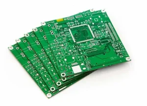
A PCB provides a physical platform for mounting electronic components and connecting them through patterned copper conductors. If you want to make a PCB yourself using a traditional subtractive process, PCB Etching is one of the classic methods for creating copper traces on a copper-clad board.
So, How to Etch a PCB?
The basic principle is relatively straightforward. A circuit pattern is transferred onto a copper-clad laminate, and the exposed copper is chemically removed using an appropriate etchant. The protected copper remains and forms the PCB traces.
After etching, the board must be cleaned, inspected, drilled where necessary, and prepared for component assembly.
DIY etching can be useful for prototypes, educational projects, and simple low-volume circuits. However, it is important to understand that professional PCB Manufacturing involves considerably more processes, including multilayer fabrication, drilling, plating, solder mask, surface finishing, electrical testing, and controlled quality inspection.
What Is PCB Etching?
PCB Etching is a subtractive PCB fabrication process that removes unwanted copper from a copper-clad substrate.
A typical DIY etched PCB consists of:
- Copper-clad laminate
- Protective circuit pattern
- Chemical etchant
- Remaining copper traces
- Drilled component holes where required
The basic process is:
PCB Design → Pattern Transfer → Copper Etching → Cleaning → Drilling → Inspection → Component Assembly
During etching, the protective pattern prevents the desired copper from being chemically removed. The exposed copper is dissolved by the etchant, leaving the circuit pattern behind.
The quality of the final PCB depends heavily on the accuracy of the transferred pattern and the control of the etching process.
PCB Layout Transfer Methods
Before starting How to Etch a PCB, you must first transfer the circuit pattern to the copper surface.
The pattern acts as an etch resist, protecting the copper that needs to remain.
Several techniques can be used for DIY PCB fabrication.
Toner Transfer
The toner-transfer method uses a laser printer to print the circuit pattern onto suitable transfer media and then transfers the toner onto the copper surface using heat and pressure.
It is relatively inexpensive and accessible, making it popular among hobbyists.
Photoresist
The photoresist method uses a photosensitive coating or film. UV light is used to expose the desired pattern, followed by development and chemical etching.
This method can provide finer features than basic toner transfer when properly controlled.
Direct Imaging or Laser Processing
More advanced systems can use laser-based patterning or direct imaging technologies to define PCB features.
These methods can provide higher precision but generally require specialized equipment and are more closely associated with professional or advanced prototyping workflows.
For simple DIY projects, Toner Transfer PCB fabrication remains one of the most accessible approaches.
How to Etch a PCB Using Toner Transfer
If you are learning How to Etch a PCB for the first time, toner transfer is a practical starting point for simple single-sided boards.
Materials and Tools
You may need:
- Copper-clad laminate
- Laser printer
- Suitable glossy transfer paper or dedicated toner-transfer paper
- PCB design software such as KiCad or EasyEDA
- Etchant
- Plastic or chemical-resistant tray compatible with the etchant
- Fine abrasive pad or suitable copper-cleaning material
- Isopropyl alcohol or another appropriate cleaning agent
- Protective gloves
- Safety goggles
- Appropriate protective clothing
- Drill and suitable PCB drill bits
For chemical handling, always follow the instructions and safety information supplied with the specific etchant.
Step 1: Design and Print the PCB Layout
Begin by designing the PCB using suitable PCB design software.
Common steps include:
- Create the schematic.
- Assign appropriate footprints.
- Complete the PCB layout.
- Check clearances and trace widths.
- Perform a design-rule check.
- Generate the appropriate fabrication artwork.
- Print the required copper layer at 1:1 scale.
For a simple single-sided toner-transfer process, the artwork orientation is critical.
Should the PCB Layout Be Mirrored?
The answer depends on which copper side is being transferred and how the transfer medium is positioned.
If the printed artwork is placed face-down onto the copper and transferred directly, the image orientation must be selected so that the resulting copper pattern has the correct orientation.
Therefore, do not blindly mirror every PCB layer. Confirm the intended transfer direction and verify text, component numbering, and connector orientation before printing.
For a DIY single-sided board, printing a small test pattern or checking the artwork against the physical board can prevent an incorrectly mirrored PCB.
Set the Printer to Actual Size
Make sure the artwork is printed at:
100% scale / Actual Size / 1:1
Do not allow the printer or PDF viewer to automatically scale the drawing to fit the page.
Even a small scaling error can affect:
- Component footprints
- Hole locations
- Connector spacing
- Trace alignment
- Component mounting
For this reason, always include a known dimension or scale reference in the printout when possible.
Step 2: Prepare the Copper-Clad Board
Cut the copper-clad laminate to the required size.
Then prepare the copper surface carefully.
Clean the Copper
Remove:
- Oxidation
- Grease
- Dust
- Fingerprints
- Surface contamination
A suitable fine abrasive pad can be used to lightly prepare the copper surface.
After abrasion, clean the board with an appropriate solvent or cleaning agent and allow it to dry completely.
Avoid touching the cleaned copper surface with bare fingers because skin oils can interfere with toner adhesion.
The objective is to create a clean, dry, uniformly prepared copper surface.
Step 3: Transfer the Toner Pattern
Place the printed artwork against the prepared copper surface according to the transfer method and paper manufacturer’s instructions.
For a heat-transfer system, controlled heat and pressure soften the toner so that it adheres to the copper.
A typical workflow is:
- Position the artwork accurately.
- Secure it to prevent movement.
- Apply the recommended heat and pressure.
- Allow the board to cool if required by the transfer process.
- Carefully remove the transfer paper.
- Inspect the transferred pattern.
Avoid relying on a single universal heating time or temperature. Different printers, papers, toners, laminates, and transfer methods behave differently.
If a toner-transfer paper manufacturer specifies a particular temperature and process, follow those instructions rather than assuming that a fixed 5–10 minute ironing time will always work.
Step 4: Inspect and Repair the Transferred Pattern
Before putting the board into the etchant, inspect the toner pattern carefully.
Check for:
- Broken traces
- Pinholes
- Incomplete toner transfer
- Unwanted bridges
- Excess toner
- Narrow traces
- Incorrect orientation
- Poor adhesion
Small defects can sometimes be corrected using a suitable permanent etch-resistant marker or another compatible resist-repair method.
This inspection step is extremely important because an error in the resist pattern will normally become an error in the final copper circuit.
Step 5: Etch the PCB
Now the board is ready for the PCB Etching stage.
Place the prepared board into a suitable chemical-resistant container containing the selected etchant.
Follow the etchant manufacturer’s instructions for:
- Concentration
- Temperature
- Exposure time
- Agitation
- Personal protective equipment
- Ventilation
- Disposal
During etching, the solution reacts with the exposed copper.
The desired copper traces remain protected, while the unprotected copper is progressively removed.
Gentle movement or appropriate agitation can help maintain fresh etchant at the copper surface and improve process consistency.
Do not rely solely on a fixed etching time. Monitor the board and remove it when the unwanted copper has been adequately removed.
Step 6: Rinse and Clean the PCB
Once the unwanted copper has been removed, carefully remove the board from the etchant according to the manufacturer’s procedure.
Rinse it thoroughly using the recommended method to stop further chemical action.
Then remove the remaining toner or etch resist using a compatible cleaning method.
Inspect the copper traces for:
- Incomplete etching
- Over-etching
- Undercut traces
- Shorts
- Open circuits
- Pinholes
- Insufficient trace width
A magnifying glass or microscope can be useful for fine traces.
Step 7: Drill the PCB
If the design uses through-hole components, drill the required component holes.
Typical DIY PCB drilling equipment includes:
- Mini rotary tool
- PCB drill press
- Appropriate carbide PCB drill bits
- Workholding fixture
Select drill sizes according to the component lead diameter and design requirements.
Take care when drilling because excessive force can:
- Break small drill bits
- Crack the laminate
- Damage nearby copper
- Create oversized holes
- Reduce mechanical reliability
For simple single-sided DIY boards, drilling is normally performed after etching.
Professional PCB fabrication uses controlled CNC drilling or laser drilling, depending on the board structure and feature requirements.
Step 8: Finish and Inspect the DIY PCB
After drilling, clean the board and inspect the entire circuit.
Check:
- Trace continuity
- Electrical isolation
- Hole positions
- Component footprints
- Solder pads
- Trace damage
- Remaining copper debris
A multimeter can be used for basic continuity and isolation checks.
Remember that a continuity test should not be interpreted blindly. A low resistance may be intentional in some parts of a circuit, so testing should be performed against the PCB schematic or netlist whenever possible.
For additional protection, a suitable solder mask or conformal coating can be considered depending on the application.
However, DIY coating methods are not equivalent to the controlled solder-mask processes used in professional PCB fabrication.
PCB Etching Solutions: Which Etchant Should You Choose?
Choosing the correct etchant is an important part of PCB Etching.
Different chemical systems have different processing characteristics, handling requirements, and waste-disposal considerations.
| Etchant | Typical Speed | Visibility | Advantages | Considerations |
|---|---|---|---|---|
| Ferric Chloride | Moderate | Dark/opaque | Widely available and established | Can stain surfaces and clothing; requires proper waste handling |
| Ammonium Persulfate | Moderate | Relatively clear | Cleaner visual process; commonly used for prototyping | Strong oxidizer; requires appropriate handling |
| Cupric Chloride | Moderate to fast when properly controlled | Variable | Can be regenerated in controlled processes | Requires careful chemical management and ventilation |
| Acid/Peroxide Systems | Can be fast | Variable | Readily available in some laboratory/prototyping environments | Can be hazardous and highly reactive; not recommended for casual handling |
There is no universally “best” PCB etchant.
Selection should consider:
- Etching rate
- Copper thickness
- Feature size
- Temperature
- Process control
- Chemical availability
- Ventilation
- Waste disposal
- User experience
For beginners, commercially formulated PCB etchants are generally preferable to improvised chemical mixtures because their handling instructions and intended applications are clearer.
Ferric Chloride vs. Ammonium Persulfate
Ferric chloride is one of the most familiar PCB etchants for hobbyists.
Ferric Chloride Advantages
- Widely available
- Established DIY process
- Relatively straightforward to use
- Suitable for basic copper etching
Ferric Chloride Disadvantages
- Dark and difficult to see through
- Can stain work surfaces and clothing
- Requires appropriate chemical waste handling
Ammonium persulfate is another common choice.
Ammonium Persulfate Advantages
- Relatively clear solution
- Easier to observe the board during etching
- Commonly used for prototype PCB processing
Ammonium Persulfate Disadvantages
- Requires appropriate chemical handling
- Reaction performance depends on concentration and temperature
- Should be stored and disposed of according to safety guidance
For beginners, the best choice is usually the commercially available etchant for which they can obtain clear handling, storage, and disposal instructions.
PCB Etching Safety Precautions
Chemical PCB etching requires appropriate safety controls.
Wear Chemical-Resistant Gloves
Use gloves that are compatible with the specific chemical being handled.
Do not assume that every glove material provides equal protection against every chemical.
Wear Safety Goggles
Eye protection is essential because chemical splashes can cause serious eye injuries.
Use Appropriate Protective Clothing
Wear suitable protective clothing or an apron to reduce skin and clothing exposure.
Provide Adequate Ventilation
Perform chemical etching in a well-ventilated area appropriate for the chemical being used.
Avoid working in enclosed living spaces.
Never use a household kitchen as a chemical etching workspace.
Avoid Direct Skin Contact
If etchant contacts your skin, follow the chemical manufacturer’s emergency instructions and rinse the affected area appropriately.
Keep Chemicals Away from Children and Pets
Store chemicals securely and clearly labeled.
Never Pour Used Etchant Down the Drain
Used etchant contains dissolved copper and must be handled as chemical waste according to applicable local regulations.
Do not dispose of it in household drains unless local authorities explicitly permit the specific waste stream.
Be Careful with Heating
Heat-transfer methods use hot equipment, while some etching processes may involve elevated temperatures.
Allow tools and PCB materials to cool safely before handling them.
Safety should always take priority over etching speed or convenience.
Common PCB Etching Problems
Even a simple DIY PCB Etching Process can produce inconsistent results.
Over-Etching
Over-etching can reduce trace width and cause undercutting beneath the etch resist.
This is particularly problematic for fine traces.
Under-Etching
If unwanted copper remains between traces, electrical shorts may occur.
Poor Toner Transfer
Insufficient adhesion can create:
- Broken traces
- Pinholes
- Open circuits
Excessive Trace Width Reduction
Etchant can attack copper laterally as well as vertically. This effect becomes more significant as etching continues.
Therefore, very fine-pitch designs can be difficult to reproduce reliably using basic toner transfer.
Incorrect Scaling
If the printed artwork is automatically resized, component holes and footprints may no longer align with the physical components.
Always verify the print scale before transfer.
DIY PCB Etching vs. Professional PCB Manufacturing
DIY etching is useful for learning and prototyping, but it has significant limitations.
| Feature | DIY PCB Etching | Professional PCB Manufacturing |
|---|---|---|
| Typical Board Type | Simple single-sided boards | Single-, double-, and multilayer boards |
| Trace Precision | Limited by process | Controlled to specified manufacturing capability |
| Plated Vias | Usually unavailable without additional processes | Standard manufacturing capability depending on design |
| Through-Hole Plating | Generally unavailable in basic DIY | Available |
| Solder Mask | Optional/manual | Controlled industrial process |
| Surface Finish | Basic exposed copper or DIY finish | ENIG, HASL, OSP, immersion tin, etc., as specified |
| Electrical Testing | Usually manual | Automated and/or fixture-based testing available |
| Production Volume | Prototype/small quantity | Prototype through mass production |
| Repeatability | Highly process-dependent | Controlled manufacturing process |
| Multilayer Capability | Difficult for basic DIY | Standard capability for qualified manufacturers |
Professional PCB fabrication is significantly more sophisticated than simply transferring a pattern and dissolving unwanted copper.
A commercial PCB Manufacturing Process may include:
Material Preparation → Inner-Layer Imaging → Etching → Lamination → Drilling → Copper Plating → Outer-Layer Imaging → Etching → Solder Mask → Surface Finish → Silkscreen → Inspection → Electrical Testing → Final Inspection
The exact process depends on the PCB structure and manufacturing requirements.
When Should You Use DIY PCB Etching?
DIY etching can be appropriate for:
- Electronics education
- Hobby projects
- Simple prototypes
- Low-complexity circuits
- Rapid experimentation
- Demonstrating basic PCB fabrication principles
It becomes less suitable when a project requires:
- Fine-pitch BGA components
- High-density interconnects
- Controlled impedance
- RF performance
- Multilayer routing
- Reliable plated vias
- High-current structures
- High-volume production
- Consistent manufacturing tolerances
- Formal reliability requirements
For these applications, professional PCB Manufacturing is generally the more appropriate approach.
How Kingda Can Support PCB Manufacturing
DIY PCB Etching is an excellent way to understand the fundamentals of copper pattern formation, but commercial electronic products normally require much tighter control over materials, dimensions, electrical performance, reliability, and production consistency.
For projects that have progressed beyond basic prototyping, Kingda can support application-specific PCB manufacturing requirements based on the customer’s design files, material requirements, stackup, dimensions, copper thickness, surface finish, and other production specifications.
Moving from a DIY prototype to a professionally manufactured PCB can help address requirements such as:
- Multilayer PCB construction
- Controlled trace geometry
- Plated holes and vias
- Solder mask
- Surface finishes
- Automated inspection
- Electrical testing
- Repeatable production
The appropriate manufacturing process should always be selected according to the actual PCB design and application requirements.
Conclusion
Learning How to Etch a PCB provides a useful introduction to the basic principles of PCB fabrication.
The fundamental process involves designing a circuit pattern, transferring that pattern to a copper-clad substrate, protecting the copper that needs to remain, chemically removing unwanted copper, and then cleaning, drilling, inspecting, and assembling the finished board.
For beginners, Toner Transfer PCB fabrication can be a practical way to explore PCB prototyping. Ferric chloride and ammonium persulfate are commonly used etchants, but the correct chemical should be selected according to handling requirements, process conditions, availability, and local waste-disposal regulations.
DIY etching is best suited to simple educational projects and prototypes. As circuit complexity increases, professional PCB Manufacturing becomes increasingly important because modern PCBs require controlled layer structures, plated vias, precise geometries, solder masks, surface finishes, electrical testing, and repeatable production quality.
Ultimately, PCB etching is more than a way to make a copper circuit at home. It provides a practical introduction to the subtractive processes behind PCB fabrication and helps engineers and hobbyists better understand how a PCB moves from a digital layout to a physical electronic circuit.