For anyone working with electronic products, PCB and PCBA are familiar terms. However, these two concepts are sometimes confused because they are closely related but represent different stages of electronic manufacturing.
What exactly is a PCB? How does it become a PCBA? What are the differences between PCB and PCBA, and how do SMT and DIP processes fit into the overall manufacturing workflow?
Understanding these concepts is essential for engineers, purchasers, and anyone involved in PCB Manufacturing and electronic product development.
What Is a PCB?
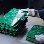
PCB, short for Printed Circuit Board, is the fundamental interconnection platform used in electronic products. A PCB provides mechanical support for electronic components and creates electrical connections between them through conductive patterns, copper layers, pads, and vias.
A bare PCB does not normally contain the electronic components themselves. Instead, it provides the physical and electrical foundation on which components can later be assembled.
Depending on product requirements, PCBs can be manufactured in many configurations, including single-sided, double-sided, and multilayer boards, as well as rigid, flexible, and rigid-flex structures.
Key Advantages of PCBs
The widespread use of PCB technology is driven by several important advantages:
-
High circuit density
Fine traces, multiple copper layers, microvias, and advanced interconnection technologies allow more circuits to be integrated into a relatively small area. This supports the miniaturization of electronic products.
-
Consistent and repeatable electrical connections
PCB layouts are manufactured according to digital design data, providing consistent circuit patterns and reducing wiring and assembly errors compared with manually wired circuits.
-
Support for automated manufacturing
Standardized PCB designs can be processed using automated imaging, drilling, plating, inspection, and assembly equipment, improving production efficiency and manufacturing consistency.
-
Standardized design and interchangeability
Standardized PCB structures and manufacturing data make it easier to reproduce the same design across production batches while maintaining consistent electrical and mechanical characteristics.
What Is PCBA?
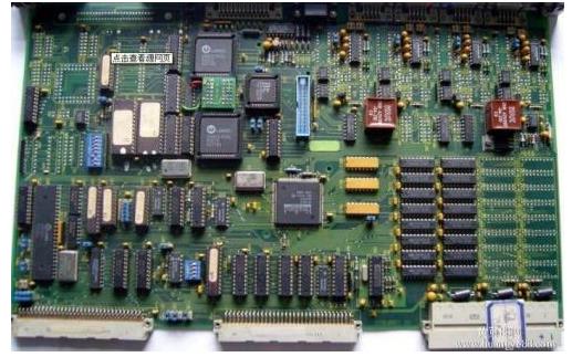
PCBA stands for Printed Circuit Board Assembly. It refers to a PCB that has undergone component assembly and soldering processes.
In simple terms:
PCB = Bare circuit board
PCBA = PCB + Electronic Components + Assembly and Soldering
A PCB becomes a PCBA after components are mounted and electrically connected to the board through an appropriate PCB Assembly process.
The assembly process may involve SMT, DIP Assembly, or a combination of both technologies, depending on the component types and product requirements.
SMT Assembly
SMT, or Surface Mount Technology, is one of the most widely used technologies in modern PCB Assembly.
Unlike traditional through-hole assembly, SMT components are mounted directly onto solder pads on the PCB surface. Their leads or terminals do not normally require component leads to pass through drilled holes.
Typical SMT components include:
- Resistors
- Capacitors
- Diodes
- Integrated circuits
- SOT and QFN packages
- BGA components
- Other surface-mount semiconductor packages
Typical SMT Process
A standard SMT production process generally includes:
PCB Loading → Solder Paste Printing → Solder Paste Inspection → Component Placement → Reflow Soldering → AOI/X-Ray Inspection → Testing and Rework
1. Solder Paste Printing
Solder paste is printed onto the PCB pads through a precision stencil. Printing quality directly affects solder joint formation, so parameters such as stencil thickness, aperture design, alignment, and solder paste volume must be carefully controlled.
2. Component Placement
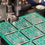
A high-speed pick-and-place machine accurately places surface-mount components onto the solder paste-covered pads.
Placement accuracy is particularly important for fine-pitch ICs, QFNs, BGAs, and other high-density packages.
3. Reflow Soldering
The populated PCB passes through a reflow oven. The solder paste is heated according to a controlled temperature profile, melts, and forms permanent solder joints between the components and PCB pads.
4. Inspection and Testing
After reflow, the board can be inspected using AOI, X-ray inspection, visual inspection, and electrical testing, depending on the product requirements.
Defects identified during inspection may require controlled rework before the assembly moves to the next production stage.
DIP Assembly and Through-Hole Components
DIP Assembly is commonly used to describe through-hole component assembly. In this process, component leads are inserted through holes drilled in the PCB and then soldered to the corresponding pads.
Through-hole technology remains useful for components that require stronger mechanical attachment, larger lead structures, or specific electrical and mechanical characteristics.
Common examples include:
- Connectors
- Switches
- Relays
- Large capacitors
- Transformers
- Power components
- Mechanically stressed components
Typical DIP Assembly Process
A typical through-hole assembly workflow may include:
PCB Preparation → Adhesive Application When Required → Component Insertion → Lead Forming/Cutting → Inspection → Wave or Selective Soldering → Cleaning → Final Inspection
The exact process depends on component structure and the required soldering technology.
Wave Soldering
Wave Soldering is commonly used when a PCB contains a relatively large number of suitable through-hole solder joints.
The PCB passes over a controlled wave of molten solder, allowing solder to contact the exposed through-hole leads and pads.
Selective Soldering
Selective soldering provides more localized soldering control. It is particularly useful for mixed-technology boards where only specific through-hole components require soldering and nearby SMT components must be protected from unnecessary thermal exposure.
PCB vs. PCBA: What Is the Difference?
The most important difference between PCB and PCBA is their manufacturing stage and physical condition.
| Item | PCB | PCBA |
|---|---|---|
| Definition | Bare printed circuit board | Assembled printed circuit board |
| Components | Normally no components installed | Electronic components installed |
| Main Process | PCB fabrication | PCB Assembly |
| SMT | Not yet performed | May be included |
| DIP Assembly | Not yet performed | May be included |
| Soldering | Generally not part of bare-board fabrication | Required for component assembly |
| Function | Provides electrical interconnection and mechanical support | Provides a completed electronic assembly |
Therefore, a PCB is the bare board used as the foundation for an electronic assembly, while a PCBA is the assembled board after components have been mounted and soldered.
How Does a PCB Become a PCBA?
The transition from PCB to PCBA involves several manufacturing stages.
A simplified process is:
PCB Manufacturing → PCB Inspection → Solder Paste Printing → SMT Placement → Reflow Soldering → Through-Hole Assembly if Required → Wave/Selective Soldering → Inspection → Testing → PCBA
Not every product requires every step. For example, an SMT-only product may not require through-hole insertion or wave soldering.
Similarly, a product containing both surface-mount and through-hole components may require a mixed-technology assembly process.
SMT, DIP, and Mixed Assembly
Modern electronic products often combine different component technologies.
SMT-Only Assembly
The board contains primarily or exclusively surface-mount components.
Typical process:
Solder Paste Printing → SMT Placement → Reflow Soldering → Inspection → Testing
This approach is widely used for compact electronic products with high component density.
Through-Hole Assembly
The board contains components installed through drilled holes.
Typical process:
Component Insertion → Inspection → Wave/Selective Soldering → Cleaning → Inspection
Mixed Assembly
A board may contain both SMT components and through-hole components.
Typical process:
SMT Assembly → Reflow Soldering → Through-Hole Insertion → Wave/Selective Soldering → Inspection → Testing
The sequence may be adjusted depending on component placement, PCB structure, soldering requirements, and production equipment.
Why the Difference Matters
Understanding the distinction between PCB Manufacturing and PCB Assembly is important when developing an electronic product.
The PCB manufacturing stage focuses on creating the board itself, including:
- Copper circuit formation
- Layer lamination
- Drilling
- Plating
- Solder mask
- Surface finish
- Electrical testing
- Dimensional and visual inspection
The PCB Assembly stage focuses on mounting and soldering components, including:
- Solder paste printing
- Component placement
- Reflow soldering
- Through-hole insertion
- Wave or selective soldering
- AOI and X-ray inspection
- Electrical testing
- Rework when required
These two stages are closely connected. PCB pad design, component spacing, solder mask design, hole dimensions, surface finish, and board flatness can all influence assembly performance.
Kingda’s Approach to PCB and PCBA Manufacturing
At Kingda, PCB fabrication and PCB Assembly are considered interconnected stages of electronic manufacturing.
A well-designed PCB should not only meet electrical requirements but also provide suitable conditions for component placement, soldering, inspection, and testing.
During PCBA production, factors such as component package type, component density, PCB thickness, thermal characteristics, soldering method, and inspection requirements should be evaluated together.
By coordinating PCB design and assembly requirements early in the product development process, manufacturers can improve production efficiency, reduce assembly defects, and achieve more consistent product quality.
Conclusion
Although PCB and PCBA are closely related, they represent different stages of electronic manufacturing.
A PCB is a bare printed circuit board that provides electrical interconnections and mechanical support for components. After components are mounted and soldered through SMT, DIP Assembly, or mixed-technology processes, the board becomes a PCBA.
As electronic products continue to become smaller, more integrated, and more complex, understanding the relationship between PCB fabrication and PCB Assembly is increasingly important.
By selecting the appropriate assembly technology and considering manufacturing requirements during PCB design, engineers can achieve better manufacturability, assembly quality, reliability, and production efficiency. Kingda provides integrated PCB and PCBA manufacturing solutions designed to support these requirements across different electronic applications.